
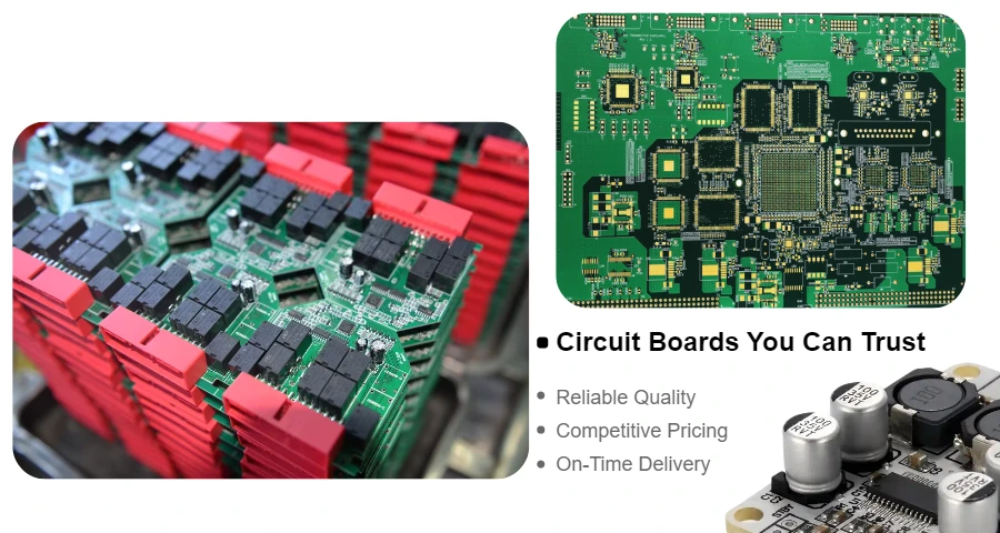
A PCB (printed circuit board) is an insulating laminated board with etched copper pathways that mechanically supports and electrically connects electronic components. Understanding what is pcb technology and the fundamental pcb meaning is essential for hardware developers, since virtually every consumer, industrial, and automotive electronic device operates on a dedicated pcb board.
By eliminating point-to-point hand wiring, printed circuit boards enable automated high-speed assembly, precise impedance control, compact mechanical packaging, and repeatable electrical performance across millions of production units.
What Is a PCB?
A PCB (printed circuit board) is a rigid, flexible, or metal-core laminated structure containing etched conductive copper traces bonded to a non-conductive dielectric substrate. To directly answer what is a pcb, it is the foundational physical platform that mechanically mounts and electrically links semiconductors, passive components, and electromechanical connectors.
In modern hardware design, a pcb board replaces brittle point-to-point wiring harnesses with photo-etched copper conductors as narrow as 3 mils (75 µm). By embedding conductive pathways within composite dielectric layers, PCBs provide predictable characteristic impedance, robust electromagnetic shielding, and automated surface-mount assembly compatibility.
What Does "PCB" Stand For? (PCB Meaning)
The exact PCB meaning stands for Printed Circuit Board.
The term "printed" originates from printing-press technology. In the 1930s and 1940s, Austrian inventor Paul Eisler adapted graphic screen-printing and chemical etching techniques to transfer electrical conductor patterns onto copper-clad insulating laminates, initially used in radio sets. While modern circuit boards are fabricated through photolithography and laser direct imaging (LDI) rather than traditional ink printing, the historical name remains universal.
Industry standards distinguish several closely related acronyms:
- PCB (Printed Circuit Board): The bare, unpopulated board containing copper traces, vias, pads, solder mask, and silkscreen before electronic components are mounted.
- PWB (Printed Wiring Board): An older synonym defined in early IPC and military standards (such as IPC-T-50 and MIL-PRF-55110) describing bare boards providing electrical interconnections without embedded active components.
- PCBA (Printed Circuit Board Assembly): The finished board once surface-mount and through-hole electronic components are soldered into place.
- PWA (Printed Wiring Assembly) / CCA (Circuit Card Assembly): Aerospace, defense, and high-reliability classifications for fully assembled, conformal-coated circuit cards installed in system chassis.
PCB vs. Circuit Board vs. PCBA (PCB Board)
Engineers and buyers frequently encounter the terms circuit board, PCB, PCB board, and PCBA used interchangeably. However, each term represents a distinct phase in electronics manufacturing.
A circuit board is the broad, generic umbrella term referring to any substrate that hosts an electrical circuit—ranging from perforated prototype stripboards and wire-wrapped breadboards to high-density rigid-flex laminates. A PCB (often colloquially called a pcb board) specifically refers to an industrially manufactured bare laminate with chemically etched copper conductors. A PCBA is the completed assembly after components have been populated and soldered.
Comparison: Circuit Board vs. Bare PCB vs. PCBA
| Feature / Aspect | Circuit Board (General) | Bare PCB (PCB Board) | PCBA (Assembled Board) |
|---|---|---|---|
| Industry Definition | Any substrate supporting electrical connections | Bare, unpopulated etched laminate with copper tracks & pads | Fully populated PCB with soldered electronic components |
| Component Population | Can be bare, hand-wired, or socketed | Zero components (bare copper, dielectric, solder mask) | Active ICs, passives, crystals, headers, connectors |
| Manufacturing Process | Hand wiring, stripboard, or factory fab | Photolithography, etching, drilling, copper plating, surface finish | SMT solder paste stencil, pick-and-place, reflow, wave soldering |
| Electrical Function | Variable depending on implementation | Passive conductive paths (open circuits between distinct nets) | Fully functional operational electronic subsystem with firmware |
| Quality Testing Method | Manual continuity probe / DMM | Automated optical inspection (AOI), flying probe electrical test (E-test) | In-circuit testing (ICT), flying probe, functional test (FCT), 3D X-ray (AXI) |
| Application Stage | Laboratory benchtop breadboarding & proof of concept | Material procurement and bare-board fab input | Final enclosure assembly, box-build, end-user deployment |
How a PCB Works (What Is PCB)
To understand how a pcb works, you must examine its multi-layered composite architecture. A printed circuit board routes electric current through engineered conductive tracks while preventing unintended shorts across insulating substrate barriers.
Core Anatomy of a PCB
- Dielectric Substrate (Core & Prepreg): The non-conductive mechanical base material. Standard boards utilize FR-4 (woven fiberglass cloth impregnated with flame-retardant epoxy resin). High-frequency RF circuits employ PTFE or hydrocarbon ceramic laminates (such as Rogers RO4350B), while heat-sensitive power systems rely on aluminum or copper metal cores.
- Conductive Copper Layers: Pure copper foil (typically 0.5 oz / 18 µm to 2 oz / 70 µm thick) laminated to the dielectric. Chemical etching removes unwanted copper, leaving precision traces that carry DC power, analog waveforms, and high-speed digital buses.
- Plated Through-Holes and Vias: Mechanically or laser-drilled holes lined with electroplated copper (20–25 µm barrel thickness) that route electrical signals vertically across multiple board layers.
- Solder Mask: A resilient liquid photoimageable (LPI) epoxy layer applied over external copper surfaces. It insulates copper tracks, shields against oxidation, and prevents solder bridges from forming between adjacent pins during automated SMT reflow.
- Silkscreen (Legend): White or colored ink printed on outer surfaces displaying component reference designators (e.g., R10, C22, U1), polarity marks, company logos, and pin-1 markers.
- Surface Finish: A protective metallic coating applied over exposed copper pads (such as ENIG, HASL, OSP, or Immersion Tin) to preserve solderability and ensure long-term contact reliability.
PCB Layer Architecture
- Single-Sided PCBs: Conductive copper on only one side of the substrate; used in cost-sensitive, low-density power supplies and household sensors.
- Double-Sided PCBs: Conductive copper on top and bottom faces, interconnected by plated through-hole vias.
- Multilayer PCBs: 4 to 64+ conductive copper layers interleaved with prepreg bonding sheets and pressed under vacuum and high heat. Multilayer construction incorporates dedicated internal ground planes and power planes for low-noise signal return paths and controlled impedance.
Frequently Asked Questions (FAQ)
What is a PCB in electronics?
In electronics, a PCB (printed circuit board) is the foundational physical carrier that mechanically mounts and electrically links semiconductors, microcontrollers, passive components, and connectors through precision-etched copper traces on an insulating dielectric substrate.
What does PCB stand for?
PCB stands for Printed Circuit Board. Historically, it is also referred to as a PWB (Printed Wiring Board). Once electronic components are soldered to it, the board is officially called a PCBA (Printed Circuit Board Assembly).
Is a PCB the same as a circuit board?
The term "circuit board" is a broad umbrella term describing any board that facilitates an electrical circuit, including breadboards and perfboards. A PCB specifically refers to an industrially manufactured board where conductors are chemically etched or photolithographically defined from laminated copper sheets.
What is the main difference between a PCB and a PCBA?
A PCB is a bare, unpopulated printed circuit board with etched copper pathways and pads, but no electronic components. A PCBA (Printed Circuit Board Assembly) is the completed board after all surface-mount and through-hole components have been placed, soldered, and inspected.
Partner with HILPCB for Rapid Turnaround PCB and PCBA Manufacturing
HILPCB provides comprehensive end-to-end PCB manufacturing solutions from quick-turn prototype fabrication to volume circuit board assembly:
- Advanced Bare-Board Capabilities: High-density interconnect (HDI), microvias, controlled impedance down to ±5%, and multi-layer rigid-flex boards up to 32+ layers.
- 100% Quality Assurance: Flying probe electrical testing, automated optical inspection (AOI), solder paste inspection (SPI), and 3D X-ray (AXI) verification.
- Rapid Prototyping & Turnkey Assembly: Complete component sourcing, SMT assembly, and functional testing delivered in as fast as 24 to 48 hours.
Contact HILPCB today to upload your Gerber and BOM files for an instant DFM analysis and competitive manufacturing quote.