
Teflon (PTFE) PCB Manufacturer | Low-Loss RF and mmWave Boards
Teflon PCB manufacturer and PTFE PCB manufacturing for RF, microwave and mmWave programs. HilPCB acts as your teflon pcb manufacturer, reviewing laminate grade, Dk/Df method, copper profile, impedance, bonding, via structure and the required TDR or VNA evidence before confirming the build.
Why Teflon/PTFE for High-Frequency PCB Designs?
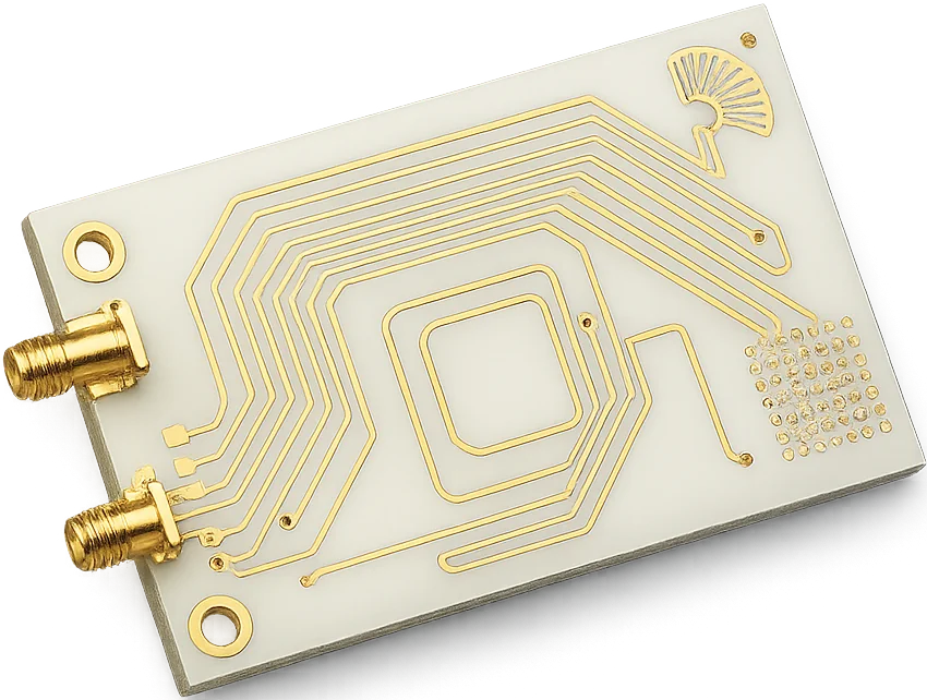
Low dielectric loss, stable Dk and predictable phaseTeflon/PTFE substrates provide low dielectric loss and stable dielectric behavior for RF, microwave and mmWave circuits. Select the laminate by the manufacturer's design Dk/Df method and frequency, not by a generic PTFE label. Compared with FR-4 PCB, these materials can provide a more predictable loss and phase baseline when the stackup and copper profile match the electrical model.
A hybrid PTFE + FR-4 stackup can place PTFE on RF layers while FR-4 supports digital, power or mechanical layers. Bonding compatibility, CTE, lamination temperature, drill behavior and registration must be reviewed together; the hybrid is a cost and construction choice, not an automatic substitute.
PTFE's low surface energy and soft mechanical behavior increase adhesion, hole-wall and dimensional risks. HilPCB reviews plasma or chemical activation, bonding films, copper profile, drill parameters, backdrill and coupon placement before release. TDR or VNA evidence is supplied when defined in the quotation and quality plan.
- PTFE and Teflon glass-reinforced options for stability
- Rolled/VLP copper to reduce roughness-induced loss
- Backdrill to residual stubs <10 mil
- TDR coupons correlated with field-solver models
- Hybrid material cost optimization
🚀 Quick Quote Request
📋 Get Full Capabilities
Fluoropolymer-Specific Manufacturing Controls
Plasma activation, staged lamination, controlled drillingPTFE/Teflon are chemically inert and require plasma activation for reliable hole-wall adhesion. We use staged temperature/pressure lamination and controlled drilling to avoid smearing. UV-laser microvias (75–100 μm) and backdrill remove resonant stubs for 25+ Gbps channels.
Verification includes TDR (±3–5% impedance), and sample-based VNA S-parameters up to 40 GHz. See high-frequency testing and impedance testing for methodology.
- Dual-stage plasma or chemical activation for adhesion
- Low-profile copper for ~10–25% lower conductor loss
- Sequential lamination for complex fluoropolymer stacks
- Coupon-based correlation with solver targets
- VNA samples to 40 GHz for RF prototypes
Teflon/PTFE PCB Technical Specifications
PTFE material, geometry and test options for RF, microwave and mmWave designs
| Decision Area | Standard Route | Advanced Review | Confirmation Basis |
|---|---|---|---|
Layer Count | 1–20 layers | Up to 40+ layers | IPC-2221 |
Base Materials | PTFE/Teflon (filled and pure), glass-reinforced | Hybrid with FR-4 / ceramic | IPC-4103 |
Board Thickness | 0.20–3.20 mm | 0.10–6.00 mm | IPC-A-600 |
Copper Weight | 0.5–2 oz | Up to 5 oz; heavy-copper path | IPC-4562 |
Dielectric Constant (Dk) | ≈2.1–2.6 @ 10 GHz | Tight-tolerance Dk lots | Material datasheet |
Loss Tangent (Df) | <0.0015 @ 10 GHz | <0.0009 @ 10 GHz | Material datasheet |
Frequency Range | Up to 40 GHz | Up to 77–110 GHz | Material dependent |
Min Trace/Space | 75/75 μm (3/3 mil) | 50/50 μm (2/2 mil) | IPC-2221 |
Impedance Control | ±7% | ±3–5% with TDR | IPC-2141 |
Surface Finish | ENIG, Immersion Silver | ENEPIG, Soft/Hard Gold | IPC-4552/4553 |
Quality Testing | 100% E-test, AOI, TDR coupons | VNA S-parameters, ionic cleanliness | IPC-9252 |
Certifications | ISO 9001, UL | AS9100, MIL-PRF-31032 (on request) | Industry standards |
Lead Time | 10–15 days | Expedite options available | Production schedule |
Need capabilities beyond this product? Explore our full manufacturing capabilities
Ready to start your PCB project?
Whether you need simple prototypes or complex production runs, our advanced manufacturing capabilities ensure excellent quality and reliability. Get your quote within 30 minutes.
RF/mmWave Design Guidelines for PTFE/Teflon
Use rolled/VLP copper to lower conductor loss by ~10–25%. Keep return-via fences within ~1× via diameter and consider backdrill so residual stubs are <10 mil. Model copper roughness in solvers and validate with coupon impedance testing. For tight space, combine with HDI microvias to control launch geometry.
PTFE laminates deliver the lowest loss available, but their softness and dimensional movement complicate processing. Where the loss budget allows a small compromise in exchange for easier fabrication and a lower price, the ceramic-filled hydrocarbon materials covered under Rogers PCB are frequently the better production choice.
Need Expert Design Review?
Our engineering team provides free DFM analysis and optimization recommendations
S-Parameter Validation & Environmental Stability
Sample-based VNA characterizes S11/S21 commonly up to 40 GHz, while TDR verifies impedance within ±3–5%. PTFE’s moisture absorption can be <0.01% for applicable grades; confirm the supplier datasheet and test method used in the electrical model. For long links or backplanes, coordinate with High-Speed PCB to budget loss and reflections.
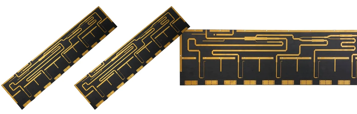
PTFE PCB Engineering Examples for RF Route Planning
These common engineering scenarios show how HilPCB can review PTFE material, copper, launch geometry and RF evidence as one released build. The RFQ defines the frequency range, fixture or reference plane, sample plan and pass/fail limits.
77 GHz radar antenna and front-end boards. Laminate grade, design Dk/Df method, copper profile, line geometry, via fences, connector launches and residual stubs must match the field model. Use the automotive radar manufacturing example to prepare impedance, backdrill and VNA inputs.
Ka/Ku-band SATCOM modules. Phase consistency, insertion loss, hybrid bonding, moisture behavior and dimensional control are reviewed with the stackup and environmental requirements. The satellite PTFE PCB example organizes those material and verification decisions.
RF test fixtures and low-loss interconnects. Connector launches, calibration planes, de-embedding and repeatable coupon geometry determine whether measured data can be compared with the model. See the high-frequency PCB testing methods when defining TDR or VNA deliverables.
Engineering Assurance & Certifications
Experience: RF builds can use coupon-to-solver correlation and material-specific lamination windows for fluoropolymers.
Expertise: the process review covers plasma activation, rolled/VLP copper selection, controlled-depth drilling and backdrill.
Authoritativeness: workflows can be aligned with IPC-6018 and quotation-defined AS9100 or MIL-PRF program documentation.
Trustworthiness: specify the required material lot, traveler, coupon and test-data traceability in the RFQ; the quotation identifies the records included with the order. See HF testing methods and advanced RF design.
Teflon and PTFE PCB RFQ Requirements
Send the latest Gerber or ODB++ package, NC drill files, fabrication drawing and proposed stackup. Identify the PTFE manufacturer and grade, approved substitutes, layer functions, finished thickness, copper profile, surface finish, quantities and delivery target.
Include the modeled Dk/Df method and frequency, impedance table, insertion-loss or phase targets, launch and backdrill details, coupon design and required TDR/VNA outputs. The listed 40+ layers, 77–110 GHz, fine-line and expedite options are not automatically combinable; engineering confirms the applicable material, geometry and test route after file review.
PTFE PCB Testing and RF Deliverables
Define acceptance evidence against the actual risk: material CoC for laminate identity, microsection for hole-wall quality, coupon TDR for impedance and sample VNA S-parameters for an agreed frequency range. Ionic cleanliness, thermal exposure or dimensional records can be added when required.
The RFQ should state method, fixture or reference plane, sample plan, limits, data format and report retention. HilPCB identifies included and optional records in the quotation so procurement can compare equivalent scopes.
Frequently Asked Questions
When should I choose PTFE/Teflon instead of Rogers or FR-4?
Do you provide S-parameter data?
How do you control via stub effects?
Which copper and finish are best for RF pads?
Can you manufacture hybrid PTFE + FR-4 or ceramic stacks?
Experience Advanced PCB Manufacturing Excellence
From simple prototypes to complex production runs, our world-class factory delivers superior quality, fast turnaround and competitive pricing. Join thousands of satisfied customers who trust us with their PCB manufacturing needs.