
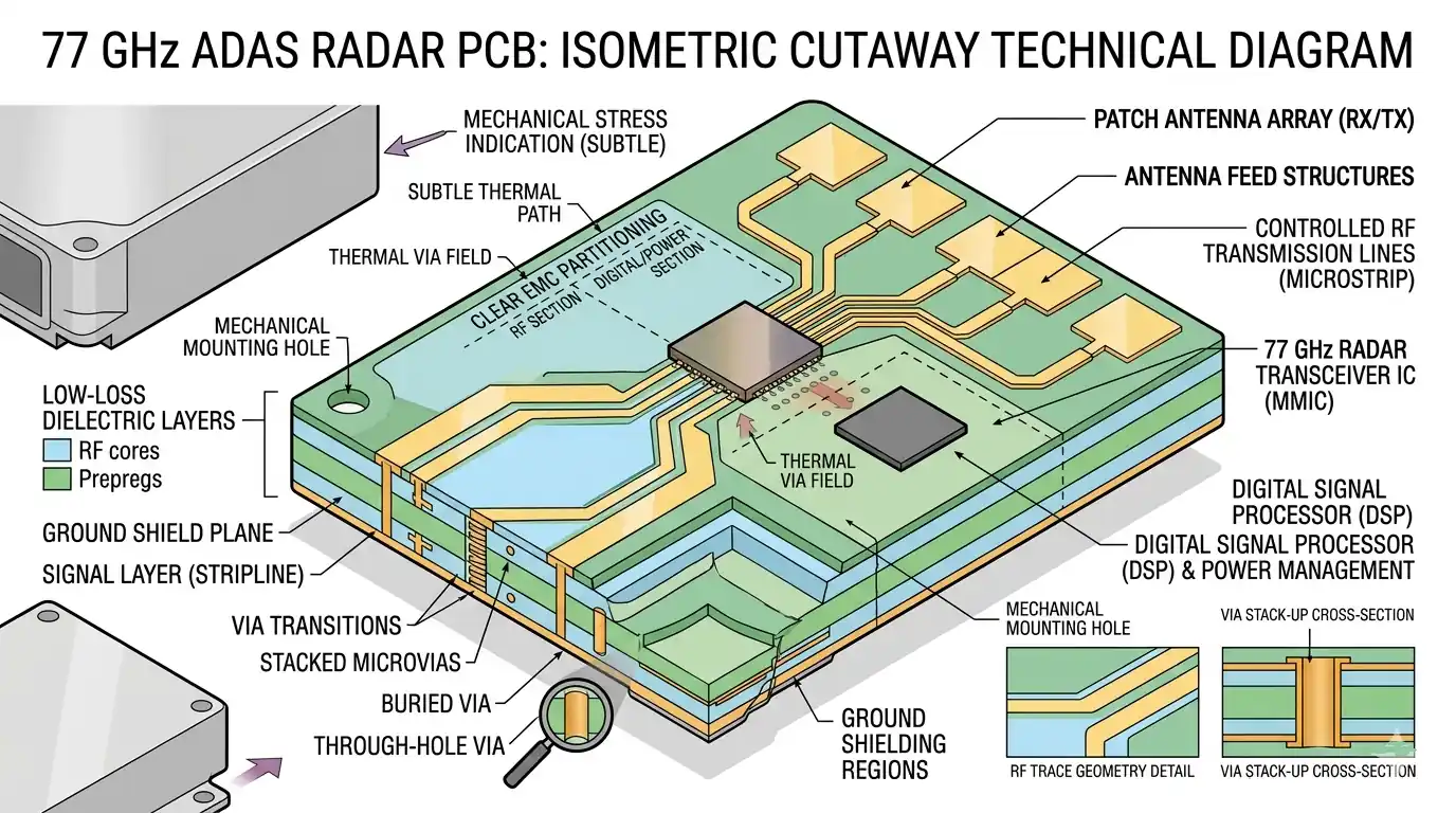
What Engineering Teams Prioritize First When Designing Automotive ADAS Radar PCBs
When designing automotive ADAS radar PCBs, the engineering team's initial priority is fundamentally not confirming single prototype metrics, but verifying whether material consistency, feed transitions, EMC boundaries, and assembly stress can be stably reproduced in mass production. For 77GHz/79GHz radar boards, what determines the project's maturity is whether this RF and manufacturing window can maintain perfect consistency across different product batches. This is because dielectric stability, stackup tolerances, shielding structures, thermal paths, and assembly stress will all directly impact the detection performance and long-term reliability of the system.
Verification Directory
- Why Automotive ADAS Radar PCBs Must Be Designed According to the 77GHz Production Window
- Automotive ADAS Radar PCB Mass Production Review Quick Reference
- How to Select Stabler 77GHz Radar Board Materials and Stackups
- Controlling Antenna Feeds, Via Transitions, and Phase Consistency
- Why Thermal Design, Shielding, and Mechanical Assembly Amplify Performance Dispersion
- Pre-planning EMC Partitioning and Return Paths for Radar Boards
- Why Assembly Yields and Test Coverage Must Be Defined Before Design Freeze
- Establishing the DFM and Verification Closed-Loop for ADAS Radar PCBs
- Frequently Asked Questions (FAQ)
- Next Steps: Initiating Automotive Radar Pre-Reviews and NPI Evaluation
Automotive ADAS Radar PCB Mass Production Review Quick Reference
| Risk Dimension | Public Literature Anchor | Project-Level DFM / RF Focus | Engineering Reminder |
|---|---|---|---|
| Operating Frequency | Automotive mmWave radars commonly operate in the 76-81 GHz band. 77 GHz / 79 GHz is the standard engineering context. |
Board-level phase consistency, localized loss, and transition tolerances are heavily amplified at mmWave frequencies. | The higher the frequency, the stricter the requirement for geometric and phase consistency. |
| Materials & Stackup | High-frequency materials and hybrid-lamination structures are frequently employed. | Dielectric thickness stability, resin systems, copper surface roughness, and lamination repeatability must be evaluated collectively. | Material batch consistency directly dictates mass production RF performance. |
| Feeds & Transitions | Local geometric variances in antenna feeds, vias, and launches directly affect reflection and phase. | Do not rely purely on nominal simulations; verify manufacturable geometry and batch-to-batch repeatability. | Feed transitions must be judged by achievable manufacturing geometry, not nominal CAD limits. |
| Assembly & Validation | Automotive applications enforce strict environmental, assemble-ability, and aging prerequisites. | Shield cans, TIMs (Thermal Interface Materials), assembly stress, and the validation matrix must be frozen early. | Automotive validation demands long-term consistency and immutable environmental stability. |
ADAS Radar PCB Risk and Freeze Point Correlation
| Most Vulnerable Stage | Typical Risk | What Needs Freezing Before Tape-out? | Downstream Penalty |
|---|---|---|---|
| Material Selection | Nominal datasheet parameters look excellent, but lamination and batch-stability fall short in execution. | Material framework, dielectric thickness, tolerances, and supply availability. | Severe gap between prototype and mass production RF deliverables. |
| Feeds & Transitions | Vias, anti-pads, and ref-plane transitions inject destructive additive reflections. | Critical feeds, layer-switching topology, return planes, and launch geometry. | Uncontrollable beam squint, massive insertion loss, or phase mismatching. |
| Thermal & Mechanicals | Shield cans, housing press-fits, and TIMs induce mechanical board warping. | Board thickness, planar tolerances, copper balance, and mechanical assembly constraints. | Severe thermal drift, batch inconsistency, and steep rework cycles. |
| Validation Release | Relying purely on basic bench function tests; missing structural and climatic validation. | RF bounds, thermal imaging, X-ray screens, microsections, and climatic stress metrics. | Systemic failures suddenly expose themselves only deep into pilot runs. |
Why Automotive ADAS Radar PCBs Must Be Designed According to the 77GHz Production Window
Automotive ADAS radar PCBs absolutely must be engineered conforming to the 77GHz mass production window because mmWave frequency bands ruthlessly amplify the impact of dielectric thickness variations, copper roughness profiles, soldermask openings, via geometry, surface finishes, and assembly-induced warpage. If these variables can only be secured on a single lab prototype but fail to replicate reliably during mass production batches, the design remains fundamentally immature.
Within the public industry context, automotive mmWave radars typically align around the 76-81 GHz band covered by ETSI TR 103 593, with 77 GHz and 79 GHz acting as the common operational framework. At the board integration level, the critical directive is not merely memorizing a frequency point, but explicitly defining that:
- These frequency bands present exponentially higher sensitivity to localized geometric deviations compared to standard high-speed digital boards.
- Successfully powering on a prototype absolutely does not guarantee that the subsequent mass production batches will maintain matching RF signatures.
- Thermal dynamics, mechanical stresses, and assembly variables translate directly into phase distortion, channel loss, and batch inconsistency issues.
- The fundamental design target must aim for stable mass-production repeatability from day one, not a mere "one-time successful bench prototype."
Therefore, the engineering starting point for an automotive radar board should never be "Let's build a board that tests well," but rigorously questioning throughout the layout phase, "Can our factory stably reproduce this exact stackup, feed matrix, and assembly scheme?"
How to Select Stabler 77GHz Radar Board Materials and Stackups
Executing a more stable material and stackup architecture for a 77GHz radar board isn't simply about extracting the lowest Dk and Df values from a datasheet. True stability lies in verifying how the material behaves under drastic temperature transients, its consistency across raw material batches, its stability under lamination pressure, and whether the fabricator possesses the competence to execute hybrid-stackups and high-frequency layers flawlessly. For automotive platforms, mass production repeatability almost always outweighs the nominal datasheet specifications of a single prototype test.
Practical engineering review methods should prioritize:
- Verifying whether the project necessitates elite High-Frequency PCB Manufacturing Capabilities or specific Rogers PCB Material Systems, rather than defaulting purely based on marketing spec sheets.
- For mixed-signal boards incorporating digital controls, power planes, and low-speed interfaces, evaluating the synergistic harmony of the Multilayer PCB Stackup Structure alongside the localized high-frequency cores.
- Scripting dielectric thickness targets, tight tolerances, and resin-flow parameters strictly into your Stackup Documentation Guide, preventing critical simulation assumptions from being lost during manufacturing handoff.
- If the radar operates under high-temperature envelopes and intense thermal aging stress over years, synchronizing High-Tg PCB Material Stability checks identically.
For automotive projects, the material configuration that actually scales into mass production is rarely the "theoretically lowest-loss option on paper," but rather the optimum matrix that balances loss characteristics, stackup consistency, and realistic factory replication capability.
Controlling Antenna Feeds, Via Transitions, and Phase Consistency
When commanding antenna feeds, via transitions, and phase consistency, the cardinal rule is treating every micro-segment—from the IC die, the package, the routing via, the feedline, through to the radiating antenna—as a strictly controlled RF structure, rather than just eyeballing the total trace length. Many project prototypes function passably, yet when transitioning to volume manufacturing, they suffer severe beam squint (deflection), spiked insertion loss, or channel mismatching. The root cause usually traces back directly to these neglected localized geometric details.
During the ECAD layout review, mandate confirmation of:
- Whether the critical feedlines propagate continuously over a completely unbroken reference plane, rigorously avoiding gap crossing, island gaps, or frequent, chaotic layer switching.
- Whether the routing vias, anti-pad clearances, and shielding ground via arrays are optimized for actual manufacturing capabilities, instead of relying purely on mathematically ideal simulation bounding boxes.
- Whether the launch zone accurately integrates the actual parasitic disturbances generated by the connector, package pads, and localized solder paste topography.
- If high-speed digital links are mixed onto the board, analyzing reference plane continuity concurrently via the High-Speed PCB Stackup and Loss Control Parameters.
Automotive radar boards are vastly different from "making sure the trace length math checks out." Operating at mmWave frequencies, geometric conformity, return path continuity, and transition repeatability consistently outweigh the relevance of nominal net lengths. Anchoring the review against the manufacturing boundaries outlined within IPC Standards confirms that this consistency inherently traces back to stackup alignment, mechanical geometric tolerance, and batch reproducibility rather than terminating merely at initial simulation results.
Why Thermal Design, Shielding, and Mechanical Assembly Amplify Performance Dispersion
Thermal design frameworks, EMI shielding structures, and mechanical assembly dramatically amplify performance dispersion because the localized heat flux densities generated by PAs (Power Amplifiers), main controllers, PMICs, and clock domains abruptly interact with the mechanical constraints enforced by shield cans, TIMs (Thermal Interface Materials), press-fit housings, and screw lockdowns. Together, these force variables distort the board's planar stress distribution and thermal gradient map. For mmWave applications, this topological distortion frequently cascades directly into impedance mismatch drift, severe gain deviation, and out-of-bounds temperature drift anomalies.
A robust NPI mass-production review aggressively questions:
- Are the thermal vias, bulk copper distribution planes, and localized thermal spreading paths immune to disruption?
- Will the critical RF zones suffer mechanical bowing or deformation after shield can soldering, rigid pressing, or housing fixation?
- Are the foundational board thickness, z-axis tolerances, and global copper balance robust enough to pin down and suppress potential heat-induced warpage?
- Have thermal simulation maps, X-ray scanning, cross-sectional micro-sectioning, and empirical temperature-rise profiling all been fused into the validation matrix?
If a project's RF output metrics exhibit massive variances before and after sealing the shielding structures, it is practically never a "test bench anomaly." It vividly signals that the physical assembly boundaries have completely failed to converge during the design closure sequence.
Pre-planning EMC Partitioning and Return Paths for Radar Boards
Automotive radar board EMC partitioning and signal return boundaries must be firmly frozen during the early design phases because resilient EMC performance originates from perfectly mapped isolation boundaries separating razor-sensitive receiving links, clock generators, rapid digital switching, and noisy power supply components—not from haphazardly pasting extra copper tape or bolting on shielding widgets as a late-stage Band-Aid. If the layout engineers fail to untangle these return boundaries natively, subsequent mitigation costs typically skyrocket. Contextualizing this within the ISO 26262 Automotive Functional Safety standard further highlights that scrambling for backend fixes will never legitimately substitute for rigorous frontend boundary mapping and closed-loop validation.
At the bare PCB layout level, finalize these components primarily:
- Do pristine, impermeable boundary zones definitively segregate the RF arrays, digital domains, power routing, and external interface clusters?
- Do the absolute critical feed lines and clock arrays command an entirely uncompromised and continuous reference ground plane?
- Have the loop inductance areas corresponding to power entries, active bias circuits, and connector zones been systematically compressed?
- Has the region enveloping connector escape routing and external wire harnesses been defensively addressed as a primary EMC radiation risk vulnerability?
For radar systems, properly configuring the layout fundamentally right the first time is exponentially cheaper and safer than lasting three brutal rounds of post-failure mitigation spins. When preparing to hand off the project to pilot manufacturing, these stringent design constraints must be formally codified within your Design Handoff guidelines and Gerber Data Preparation Protocols.
Why Assembly Yields and Test Coverage Must Be Defined Before Design Freeze
SMT assembly yields and electrical test coverage parameters must be explicitly defined leading up to the design freeze because automotive ADAS radar boards routinely integrate dense, fine-pitch BGAs, heavy shield cans, fragile mmWave connectors, coaxial interfaces, or highly asymmetrical hybrid-solder structures. If the engineering intent solely fixates on theoretical RF performance while ignoring solder joint volume consistency, BGA coplanarity limits, SMT reflow thermal windows, and test-point accessibility, the project will predictably be strangled by abysmal assembly yields and massive batch-to-batch dispersion during trial runs.
When transitioning to NPI manufacturing, comprehensively verify:
- Whether the layout explicitly aligns with the targeted SMT Assembly Capabilities or Turnkey Assembly Frameworks ahead of time.
- Are the stencil aperture designs, localized solder paste volumetric allocations, and the specific reflow oven profiling (recipe) individually audited specifically for the shield cans, complex connectors, and ultra-high-frequency components?
- Are the exact Bill of Materials (BOM), component polarities, specialized placement restrictions, and critical part tracking requirements locked securely into the Assembly BOM guidelines?
- Will the testing strategy guarantee not only power-on capabilities and basic functions, but also detect manufacturing process drift and batch deviations instantly on the factory floor?
A predominant number of radar board crises don't arise because the board "cannot be built," but because once produced, the batch dispersion is uncontrollably wide, and the manual rework burden is cripplingly expensive. These systemic issues are almost universally embedded into the system straight from the pre-freeze design phase.
Establishing the DFM and Verification Closed-Loop for ADAS Radar PCBs
Successfully constructing the DFM and validation closed-loop for automotive ADAS radar PCBs hinges entirely on lashing the design intents, the manufacturing process windows, and the verification mechanisms into a single, unified release logic. R&D, fabrication, and final testing must not be allowed to pursue isolated KPIs. The only valuable release metric guarantees that the RF tolerances, thermal maps, assembly mechanics, and climatic endurance boundaries are simultaneously secured within the identical traceable closed loop, rather than prematurely celebrating that "the lab prototype achieved power-on."
A robust pre-release (tape-out) checkpoint sequence incorporates:
- Stackup and Material Freeze: Have the specific dielectric matrix, exact copper surface profile, surface finish, and critical impedance tolerances been explicitly signed off by the fabricator?
- Critical RF Structure Freeze: Have the feed traces, inter-layer transitions, launch fields, and EMI shield boundaries survived mass-production oriented DFM scrutiny?
- Mechanical Assembly Constraint Freeze: Have the pressing constraints correlating to shield cans, TIM allocations, connectors, and housings been permanently anchored into the manufacturing dataset?
- Data Handoff Integrity: Are the release packages immaculately sanitized according to the PCB Manufacturing Handoff Prerequsites, the Gerber Data Preparation Directives, and the Design Handoff Blueprint Guidelines?
- Validation Matrix Freeze: Are RF extraction, thermal profiling, cosmetic AOI, destructive microsectioning, 3D X-ray, and climatic environmental stresses system-wide integrated into the Reliability Test Matrix?
- Trial Run Panelization Strategy Freeze: If the board outline is highly asymmetrical or highly sensitive to post-routing stress, re-verify the mass production limits using PCB Panelization Design Guides.
The immense value of deploying this closed loop is transforming the radar board's performance control parameter from acting on "hope and experience" to executing strictly on "process control data." Pilot manufacturing ramp-up periods accelerate dramatically, and immutable batch-to-batch consistency is achieved exponentially faster.
Frequently Asked Questions (FAQ)
Q: Is selecting ultra-low-loss materials the only requirement to ensure an automotive radar board works?
A: No, that is insufficient. Low loss materials serve solely as the baseline foundation. What determines mass production stability includes dielectric thickness tolerances, the copper foil roughness profile, stackup lamination consistency, via geometric transitions, assembly stress mitigation, and the applied verification methodology.
Q: Why do early prototypes easily pass bench testing, yet subsequent mass production batches suffer from severe RF performance drift?
A: The typical defect lies in failing to define the strict mechanical process window upfront. Microscopic material batch variations, lamination pressure tolerances, slightly shifted solder topography, shield can assembly stress, and altered thermal dissipation paths combine to inflict critical RF divergences between the volume production boards and the initial lab prototype.
Q: Can ADAS radar board EMC issues be resolved efficiently with post-layout shielding add-ons?
A: Generally, no—they cannot be entirely resolved this way. Add-on shielding components only pacify localized radiation leakage points. stable EMC performance remains irreversibly dependent on early-stage layout partitioning, unbroken return paths, and optimal connector zone signal escape mapping.
Q: Which design elements must be frozen absolutely first before scaling a radar board into mass production?
A: Prioritize locking down the material sets, precise stackup matrix, RF feed routes, via transitions, shield boundaries, thermal interface locations, SMT assembly windows, test coverage density, and the reliability verification matrix. Permitting any of these variables to drift late in the timeline guarantees catastrophic rework costs during pilot runs.
Q: Why does mechanical assembly actively degrade or shift mmWave radar performance?
A: Installing shield cans, bolting on solid heatsinks, press-fitting housings, and applying screw torque systematically alter the intrinsic physical stress state and contact interfaces across the PCB surface. Operating in the mmWave spectrum, these minute mechanical deformations distort geometric boundaries, instantly translating into catastrophic impedance shifts and phase inconsistencies.
Next Steps: Initiating Automotive Radar Pre-Reviews and NPI Evaluation
If your engineering divisions are accelerating the deployment of 77GHz/79GHz automotive radar modules, forward-facing radar systems, corner radars, or parallel high-frequency RF control electronics, the most effective preventative action isn't asking the fabricator "Can you build this board?". A highly secure launch requires pulling the following data vectors simultaneously into a comprehensive DFM pre-review:
- The final Stackup definition, explicitly chosen material architecture, and key manufacturing tolerances.
- The RF Feedline geometry, the specific via transition mapping, and critical RF transmission zone structures.
- EMI Shielding, Thermal routing, structural housing, and the defined SMT assembly process window.
- The First Article Inspection (FAI) plan, environmental stress matrix, and the parameters for evaluating batch-to-batch consistency.
Synchronizing these datasets closely with High-Frequency PCB Manufacturing Parameters, Stackup Documentation Checks, the Design Handoff Blueprint, and the rigid Reliability Test Matrix Baseline ensures you can swiftly demarcate which boundaries operate within standardized public framework capabilities, and which nodes require hyper-strict, custom DFM and RF isolations exclusively for your project.
To execute a comprehensive stackup alignment review, an RF feed transition audit, or a mass production DFM viability assessment prior to freezing your automotive radar design, directly Connect with the PCB Engineering Team to parameterize your exact layout objectives.
Advanced DFM Engineering Research Resources:
- PCB Stackup Documentation Guide
- PCB Design Handoff guidelines
- Gerber Data Preparation Parameters
- PCB Reliability Testing Matrices
- SMT Assembly BOM Management guidelines
*Author: HILPCB High-Speed Interconnect Engineering Team* *Reviewed by: HILPCB SI/DFM Engineering Team* *Last Updated: 2026-04-04*