
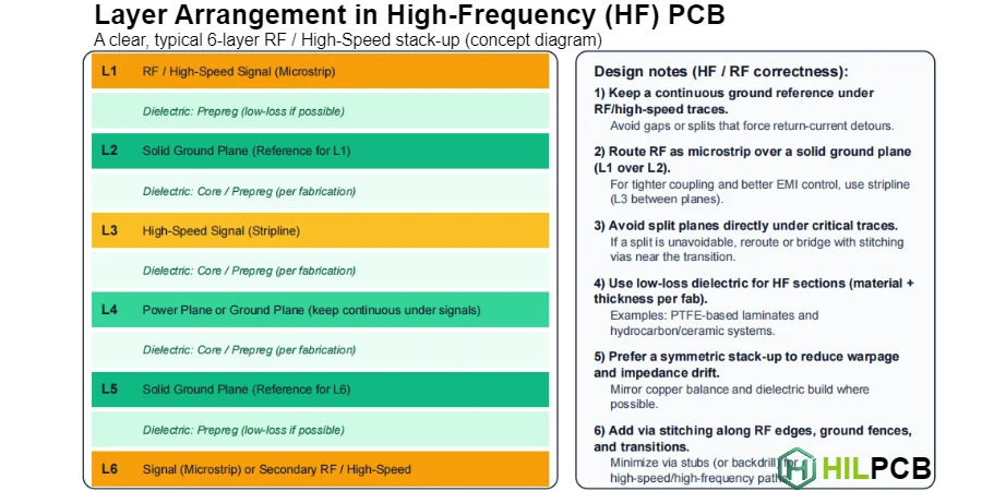
Layer arrangement—the specific ordering of signal, ground, and power layers—determines how effectively a stackup supports high frequency signals. The same number of layers arranged differently can yield dramatically different performance. Optimal arrangement provides each signal class with appropriate reference planes, routing flexibility, and isolation from noise sources.
This guide provides practical strategies for arranging layers in high frequency PCB designs, from basic principles to complex multi-layer configurations.
HILPCB manufactures high frequency PCBs with optimized layer arrangements, providing engineering support to help customers achieve optimal signal integrity through proper layer ordering.
Principles of HF Layer Arrangement
Effective layer arrangement follows electromagnetic principles that govern high frequency signal behavior. Understanding these principles enables informed decisions about layer ordering.
At HILPCB, our engineering team reviews customer stackups against these principles, recommending optimizations before manufacturing.
Signal-Reference Pairing
Every high frequency signal layer must have an immediately adjacent reference plane. This is the most fundamental principle—violating it guarantees signal integrity problems. At high frequencies, return current flows directly beneath the signal trace through the adjacent plane. Without this plane, return current takes unpredictable paths, creating noise and EMI.
Solid Plane Requirement
Reference planes must be continuous beneath signal traces. Splits, gaps, and cutouts force return current to detour, adding inductance to the signal path. When planes must be split (for power domains), never route high frequency signals across the split boundary.
Multiple Reference Options
Stripline configuration places signals between two planes, providing references above and below. This offers several advantages: reduced radiation, lower crosstalk, symmetric field distribution. When both planes are ground, the signal sees the parallel combination as reference.
Layer Pair Concept
Think in terms of layer pairs rather than individual layers. A signal layer and its reference plane form a functional unit. Additional signal layers need additional planes. This pairing concept drives layer count decisions—each signal layer pair requires associated plane layers.
Isolation Through Separation
Physical distance between signals provides isolation. Sensitive signals can be placed on distant layers to minimize coupling. Ground planes between signal layers act as shields, blocking both electric and magnetic field coupling.
Signal Layer Positioning Strategies
Where signal layers appear in the stackup affects their performance characteristics and routing suitability. Different positions suit different signal types.
HILPCB DFM review validates that signal layer assignments align with frequency requirements and routing constraints.
Outer Layers (Microstrip)
Outer layers provide microstrip configuration:
- Direct component access without vias
- Easier inspection and rework
- Some field exposure to air
- Potential radiation at high frequencies
Best for: component connections, moderate frequency signals, short critical runs where via avoidance matters.
Inner Layers (Stripline)
Inner layers provide stripline configuration:
- Complete shielding by surrounding planes
- No radiation, reduced crosstalk
- Via required for component access
- More predictable impedance
Best for: critical HF signals, long traces, differential pairs requiring isolation, signals above 5 GHz.
Near-Surface Inner Layers
Layers immediately inside the outer planes offer compromise:
- Short via stubs to reach components
- Better shielding than microstrip
- Moderate frequency performance
Best for: high-speed signals that need some component proximity.
Deep Inner Layers
Layers near stackup center:
- Maximum shielding
- Long via stubs (may need back-drilling)
- Most isolated from external coupling
Best for: most sensitive signals, clock distribution, critical analog.
Signal Layer Position Guidelines
Ground and Power Plane Ordering
The arrangement of ground and power planes significantly affects both signal integrity and power distribution quality. Proper ordering supports both functions.
At HILPCB, stackup review includes plane ordering assessment with recommendations for optimal arrangement.
Ground Planes First
In most designs, prioritize ground planes as signal references:
- Ground is quieter than power (no switching noise)
- Ground connects directly to component returns
- Multiple ground planes can parallel for lower impedance
- Ground planes provide shielding between sections
Power Plane Positioning
Power planes serve two functions—power distribution and signal reference. When used as reference, power planes must be adequately decoupled to appear as AC ground.
Position power planes where:
- Decoupling capacitors can connect efficiently
- Power distribution reaches all loads
- Switching noise won't couple to sensitive signals
Ground-Power Pairs
Adjacent ground and power planes form a distributed capacitor that helps decouple the power system:
- Closer spacing increases capacitance
- Thin dielectric (~2-4 mils) recommended
- Position pair near high-current loads
- Provides high-frequency decoupling
Multiple Power Domains
Designs with multiple supply voltages need careful plane arrangement:
- Each voltage may need dedicated plane or plane area
- Keep high-current switching supplies away from sensitive signals
- Consider split planes vs. multiple full planes
- Ensure each domain has adequate decoupling
Isolation Planes
Ground planes between signal layers provide isolation:
- Signal-Ground-Signal: Some isolation
- Signal-Ground-Ground-Signal: Better isolation
- Dedicated isolation ground: Maximum separation for sensitive signals
Adjacent Layer Coupling Considerations
Signals on adjacent layers can couple to each other, creating crosstalk. Layer arrangement must account for and minimize this coupling.
HILPCB engineering can provide coupling analysis for critical layer pairs when requested.
Broadside Coupling
When signal layers are immediately adjacent (no plane between), broadside coupling occurs:
- Traces stacked directly can couple strongly
- Orthogonal routing reduces coupling significantly
- Same-direction routing maximizes coupling
- Use only when coupling is acceptable or desired (differential pairs)
Diagonal Coupling
Traces at angles other than parallel or orthogonal:
- Coupling less than parallel, more than orthogonal
- Difficult to predict and control
- Avoid for critical signals
Orthogonal Routing Strategy
When adjacent signal layers exist without intervening plane:
- Route horizontally on one layer, vertically on adjacent
- Crossing traces couple minimally
- Parallel runs violate orthogonality—keep short
- This is standard practice for inner layer pairs
Plane-Separated Layers
Signal layers separated by ground plane:
- Coupling dramatically reduced
- Routing direction less constrained
- Preferred for crosstalk-sensitive signals
- May require additional layers in stackup
Practical Layer Arrangement Examples
Concrete examples illustrate how principles apply to real stackup decisions.
4-Layer Standard Arrangement
Layer 1: Signal (microstrip, component side) Layer 2: Ground (reference for L1) Layer 3: Power (reference for L4, decoupling with L2) Layer 4: Signal (microstrip, solder side)
This arrangement provides solid references for both signal layers. Route highest frequency signals on L1 where ground reference is adjacent.
6-Layer High-Speed Arrangement
Layer 1: Signal (microstrip) Layer 2: Ground Layer 3: Signal (stripline, orthogonal to L4) Layer 4: Signal (stripline, orthogonal to L3) Layer 5: Power Layer 6: Signal (microstrip)
Critical HF signals route on L3/L4 as stripline with ground above. L3 and L4 use orthogonal routing. Components on L1/L6 with short transitions to inner layers.
8-Layer Isolated Arrangement
Layer 1: Signal Layer 2: Ground Layer 3: Signal (critical HF) Layer 4: Ground (isolation) Layer 5: Power Layer 6: Signal Layer 7: Ground Layer 8: Signal
L3 gets dedicated ground reference above and below (L2, L4). Most critical signals route here with maximum isolation.
10-Layer Mixed Signal
Layers 1-2: Digital microstrip + ground Layers 3-4: Digital stripline pair + power Layers 5-6: Ground-ground isolation barrier Layers 7-8: Analog stripline pair + power Layers 9-10: Analog microstrip + ground
Physical separation plus double-ground barrier isolates analog from digital.
Related Layer Structure Topics
- High Frequency PCB Layer Structure: Complete stackup design guide
- Ground Plane Design for HF PCB: Ground plane optimization techniques
- Power Plane Design for HF PCB: Power distribution in HF designs
- Layer Coupling in High Frequency PCB: Managing interlayer coupling
- Stack Balance in HF PCB: Achieving symmetric construction
HILPCB Layer Arrangement Services
HILPCB delivers manufacturing precision for optimized layer arrangements:
Stackup Review: Engineering assessment of proposed layer arrangement with optimization recommendations for your signal requirements.
Flexible Configurations: Support for standard through complex arrangements with up to 20+ layers and controlled impedance on any layer.
Process Capability: Consistent layer-to-layer registration (±15-25 μm) ensures accurate interlayer relationships.
Verification: Cross-section analysis available to verify actual layer positions match design intent.
From prototypes through production, HILPCB maintains layer arrangement accuracy for high frequency applications.
Contact HILPCB for layer arrangement review and manufacturing quotation.
Common Questions
Why is layer arrangement important in high frequency PCB design?
The order of signal, ground, and power layers determines return paths, coupling, isolation, and how easily critical traces can be controlled.
Can two boards with the same layer count perform differently?
Yes. The same number of layers can behave very differently if reference planes, spacing, and routing layers are arranged differently.
What role do ground planes play in HF layer arrangement?
Continuous ground planes provide stable reference paths, improve impedance control, and reduce crosstalk and radiation.
How is a good HF layer arrangement selected?
It is chosen by balancing signal containment, isolation, manufacturability, power distribution, and the routing needs of the actual design.