
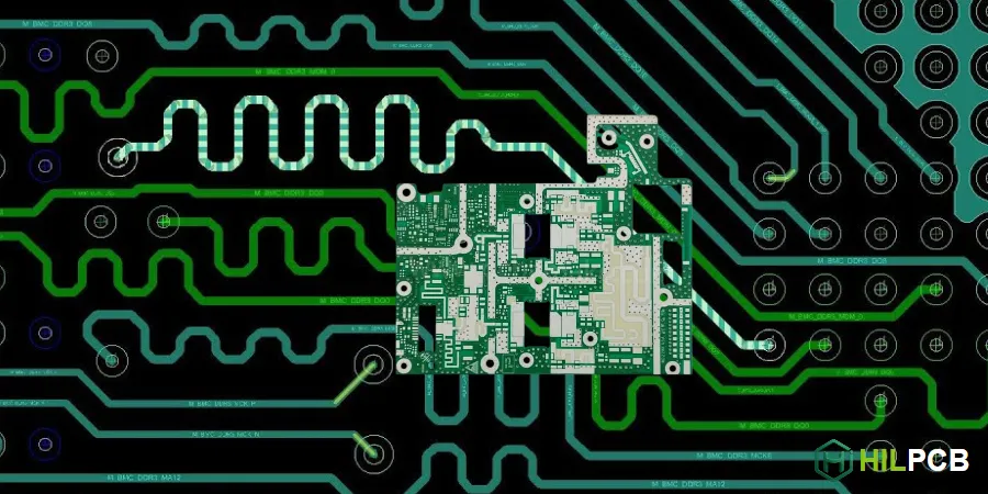
Signals on different PCB layers can interact through electromagnetic coupling—a phenomenon that increases in significance with frequency. This interlayer coupling can transfer noise between circuits, create unexpected crosstalk paths, and affect signal integrity in ways that same-layer analysis doesn't reveal. Understanding and controlling layer coupling is essential for successful high frequency design.
This guide provides practical knowledge for managing layer coupling in high frequency PCBs, from understanding coupling mechanisms to implementing effective isolation.
HILPCB manufactures high frequency PCBs with controlled dielectric properties and precise layer spacing that enable predictable coupling behavior and effective isolation.
Understanding Interlayer Coupling Mechanisms
Electromagnetic fields don't stop at layer boundaries. Signals on one layer create fields that extend into adjacent layers, potentially affecting signals routed there. Understanding these coupling mechanisms enables designs that control or minimize unwanted interaction.
At HILPCB, our engineering team can provide coupling analysis for critical layer combinations when requested.
Electric Field Coupling (Capacitive)
Voltage on one conductor creates an electric field that terminates on nearby conductors. When conductors on adjacent layers are close, significant capacitive coupling occurs:
- Coupling increases with area overlap
- Coupling increases as layers get closer
- Coupling increases with dielectric constant
- High-impedance nodes are more susceptible
Magnetic Field Coupling (Inductive)
Current flow creates magnetic fields that encircle the conductor. These fields can induce voltage in conductors on adjacent layers:
- Coupling increases with current magnitude
- Coupling depends on loop orientation
- Parallel currents couple more than perpendicular
- Low-impedance loops are more susceptible
Via Coupling
Vias provide vertical coupling paths between layers:
- Via barrel couples to adjacent traces on transition layers
- Via anti-pads in planes create field discontinuities
- Multiple vias in proximity can couple to each other
- Via stubs create resonant coupling structures
Plane-Mediated Coupling
Plane layers can transfer noise between circuits:
- Return currents in planes spread beyond signal paths
- Overlapping return current regions couple signals
- Plane resonances can distribute noise across board
Coupling Between Signal Layers
When two signal layers are positioned close together, signals on each layer can affect the other. Managing this coupling requires understanding when it occurs and how to minimize it.
HILPCB DFM review identifies potential signal layer coupling issues based on stackup and routing patterns.
Adjacent Signal Layer Coupling
Signal layers immediately adjacent (no plane between) have the strongest coupling:
- Traces directly above/below each other couple strongly
- Parallel routing amplifies coupling
- Crossing traces couple minimally
- Typical coupling coefficient: -20 to -30 dB without precautions
Orthogonal Routing Strategy
The standard mitigation for adjacent signal layers:
- Route one layer horizontally, adjacent layer vertically
- Traces cross at 90°, minimizing coupling
- Parallel runs eliminated by direction constraints
- Effective reduction: additional 10-20 dB isolation
Layer Coupling Reduction Techniques
Plane-Separated Signal Layers
Ground plane between signal layers provides shielding:
- Electric fields terminate on plane
- Magnetic fields largely blocked
- Coupling reduced by 40-60 dB typically
- Most effective for sensitive signal isolation
Separation Distance Effects
Greater physical separation reduces coupling:
- Coupling decreases approximately with distance squared
- Each doubling of distance reduces coupling ~6 dB
- Practical limit: increased layer count and cost
Coupling to and Through Power Planes
Power planes participate in coupling through their role as signal references and through their own noise characteristics.
At HILPCB, we provide guidance on power plane coupling management as part of stackup review services.
Power Plane as Coupling Path
When signals reference power planes:
- Power plane noise directly affects signal quality
- Multiple signals sharing power reference can couple through it
- Switching currents create voltage variations
- Sensitive signals should reference ground when possible
Power-to-Signal Coupling
Noise on power planes can couple to nearby signal layers:
- Closer signal-to-power spacing increases coupling
- High-frequency switching noise couples most readily
- Filtering and decoupling reduce coupling source
- Increased ground plane shielding can help
Interplane Coupling
Power and ground plane pairs couple to each other:
- This coupling provides desired decoupling capacitance
- Resonances in the cavity can enhance coupling at specific frequencies
- Edge effects create radiation and coupling at board periphery
- Via stitching along edges reduces edge effects
Mitigating Power Plane Coupling
Reduce unwanted coupling from power planes:
- Adequate decoupling to minimize plane voltage variations
- Use ground planes for signal reference when possible
- Maintain distance between signals and power plane edges
- Filter power at point of entry to sensitive circuits
Broadside Coupled Differential Pairs
Broadside coupling intentionally couples traces on adjacent layers for differential pair implementation. This technique uses layer coupling constructively.
HILPCB manufactures broadside-coupled differential pairs with precise layer registration for balanced coupling.
Broadside vs. Edge Coupling
Edge coupling: Both traces on same layer, side by side Broadside coupling: Traces stacked on adjacent layers, one above the other
Broadside Advantages
- Saves horizontal routing space
- Tighter coupling possible than edge-coupled
- Better isolation from adjacent single-ended signals
- Symmetric field distribution through dielectric
Broadside Challenges
- Requires precise layer registration (±1-2 mils)
- Layer thickness variation affects coupling
- More sensitive to manufacturing variation
- Via transitions affect pair balance
Implementation Guidelines
For successful broadside coupling:
- Specify tight registration tolerance
- Match via structures for both traces
- Maintain consistent dielectric between layers
- Verify coupling through impedance testing
Controlling Unwanted Coupling
Practical techniques for reducing layer coupling where it's not wanted.
HILPCB DFM review includes coupling assessment for sensitive designs.
Stackup Design Choices
Build isolation into the stackup:
- Separate sensitive signal groups on distant layers
- Place ground planes between signal layer groups
- Use dedicated isolation planes where needed
- Minimize adjacent signal layer occurrences
Routing Strategies
Route to minimize coupling:
- Maintain orthogonal routing on adjacent layers
- Avoid parallel runs when crossing between layers
- Keep sensitive traces away from via fields
- Use guard traces with stitching for critical signals
Via Management
Reduce via-related coupling:
- Minimize via count on sensitive nets
- Use back-drilling to reduce via stub coupling
- Place ground vias near signal vias
- Avoid via clusters near sensitive signals
Shielding Structures
Add shielding when other methods are insufficient:
- Via fences between sensitive regions
- Embedded ground grids in signal layers
- Shielding cans over sensitive components
- Guard rings around sensitive areas
Design Verification
Verify coupling performance before manufacturing:
- 3D electromagnetic simulation for critical areas
- Coupling analysis in signal integrity tools
- Test vehicle verification for new stackup configurations
- Post-manufacturing measurement of coupling
Related Layer Structure Topics
- High Frequency PCB Layer Structure: Complete stackup design guide
- Layer Arrangement in HF PCB: Signal and plane ordering strategies
- Ground Plane Design for HF PCB: Ground plane optimization techniques
- Power Plane Design for HF PCB: Power distribution in HF designs
- Stack Balance in HF PCB: Achieving symmetric construction
HILPCB Layer Coupling Services
HILPCB delivers manufacturing precision for controlled coupling behavior:
Registration Accuracy: ±15-25 μm layer-to-layer registration for predictable coupling in broadside structures and consistent isolation.
Dielectric Control: Consistent dielectric thickness and properties for uniform coupling characteristics across production.
Shielding Support: Dense via stitching capability for effective shielding structures and isolation barriers.
Analysis Support: Engineering consultation on coupling concerns with stackup optimization recommendations.
From prototypes through production, HILPCB provides controlled coupling for high frequency applications.
Contact HILPCB for layer coupling review and manufacturing quotation.