
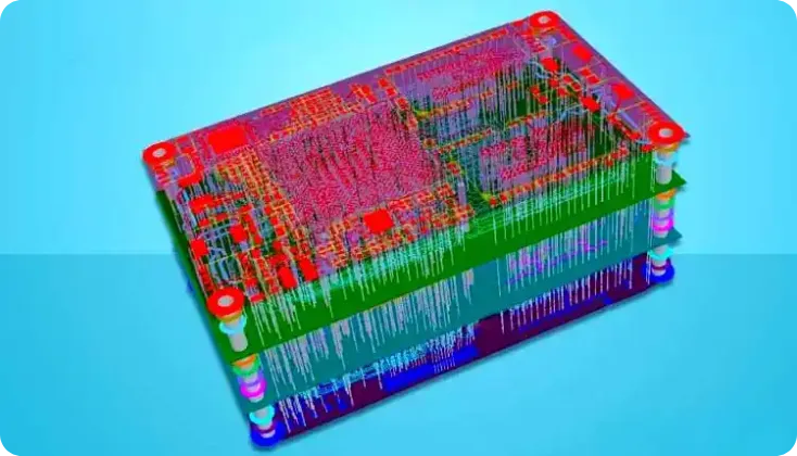
Balanced stackup construction prevents warpage and ensures consistent electrical performance in high frequency PCBs. An unbalanced stackup can twist, bow, or cup during manufacturing and thermal cycling, creating assembly problems and potentially affecting impedance. For HF designs where precise geometry determines signal integrity, stack balance is not optional—it's a fundamental requirement.
This guide provides practical knowledge for designing balanced stackups that remain flat and stable throughout manufacturing and product life.
HILPCB manufactures high frequency PCBs with balanced construction verified through our lamination process, achieving flatness specifications suitable for demanding assembly requirements.
Why Stack Balance Matters
Unbalanced stackups create internal stress during manufacturing that manifests as board warpage. This warpage affects both manufacturing and long-term reliability.
At HILPCB, our engineering team reviews stackup balance as part of standard DFM analysis, recommending adjustments to achieve flat, stable boards.
Manufacturing Temperature Cycling
During lamination, the board heats to cure prepreg materials (typically 180°C or higher). Different materials expand differently with temperature. When the board cools, unbalanced construction creates internal stress as materials try to contract to different extents. This stress causes the board to warp.
Assembly Challenges
Warped boards create assembly problems:
- Components don't sit flat on pads
- Solder paste doesn't distribute evenly
- BGA connections may not form properly
- Pick-and-place accuracy degrades
- Reflow can worsen warpage
Long-Term Reliability
Internal stress from unbalanced construction can:
- Cause delayed warpage over time
- Create via barrel stress
- Affect solder joint reliability
- Change impedance with temperature cycling
High Frequency Specific Concerns
HF designs are particularly sensitive:
- Dielectric thickness changes affect impedance
- Via connections may stress
- Differential pairs may become unbalanced
- Connector interfaces may deform
Symmetric Layer Structure Design
Symmetry around the board centerline is the primary strategy for achieving balanced construction. A perfectly symmetric stackup experiences equal forces on both sides during thermal cycling.
HILPCB supports both symmetric and asymmetric constructions, with clear communication about expected flatness for each approach.
Mirror Image Construction
The ideal balanced stackup mirrors exactly around the center:
- Same material types above and below center
- Same dielectric thicknesses
- Same copper weights
- Same layer functions (plane vs. signal)
Example 8-Layer Symmetric Stackup
Layer 1: 1 oz copper (signal) Prepreg: 4 mil FR-4 Layer 2: 1 oz copper (ground plane) Core: 8 mil FR-4 Layer 3: 0.5 oz copper (signal) Prepreg: 4 mil FR-4 ---CENTER--- Prepreg: 4 mil FR-4 Layer 4: 0.5 oz copper (signal) Core: 8 mil FR-4 Layer 5: 1 oz copper (power plane) Prepreg: 4 mil FR-4 Layer 6: 1 oz copper (signal)
Stack Balance Checklist
Hybrid Material Symmetry
When using different materials (FR-4 with Rogers, for example), maintain symmetry:
- If using Rogers on one signal layer, use it on the mirrored layer
- Match CTE (coefficient of thermal expansion) across centerline
- Consider material stiffness differences
Odd Layer Count Considerations
Odd layer counts are inherently asymmetric but can be balanced:
- Center layer acts as symmetry axis
- Layers above and below should mirror
- Center layer material choice affects overall balance
Copper Balance Strategies
Even with symmetric layer arrangement, uneven copper distribution causes warpage. Copper and dielectric have different CTEs—areas with more copper behave differently than areas with less.
HILPCB provides copper balance analysis and can recommend fill patterns to achieve better balance.
Copper Coverage Assessment
Evaluate copper coverage on each layer:
- Large ground/power planes: ~90%+ coverage
- Dense signal routing: ~50-70% coverage
- Sparse routing: ~20-40% coverage
Top-to-Bottom Balance
Compare total copper on top half vs. bottom half:
- Sum copper weight × coverage for each layer
- Compare top half total vs. bottom half total
- Imbalance creates bowing (concave toward light copper side)
Left-to-Right and Area Balance
Uneven distribution across the board area causes twisting:
- Concentrated copper in one area vs. distributed
- Different routing density in different board regions
- Component placement affecting local copper density
Copper Fill for Balance
Add copper fill to sparse areas:
- Thief copper in open areas
- Cross-hatched ground fill
- Fill connected to ground or floating (with via connections)
- Match fill patterns on mirrored layers
Copper Fill Guidelines
- Maintain minimum spacing from signals (crosstalk consideration)
- Connect fill to ground with adequate vias
- Use consistent fill pattern on balanced layers
- Avoid fill islands (unconnected copper)
Material Matching and CTE Considerations
Different materials expand at different rates with temperature. Matching materials or understanding CTE differences enables balanced construction.
HILPCB maintains material specifications including CTE data for proper stackup engineering.
CTE Basics
Coefficient of thermal expansion (CTE) measures dimensional change with temperature:
- FR-4 x-y CTE: ~12-16 ppm/°C
- Rogers 4350B x-y CTE: ~11-14 ppm/°C
- Copper CTE: ~17 ppm/°C
- Z-axis CTE varies more (affects via stress)
Material Matching Strategy
For best balance:
- Use same material family throughout when possible
- If mixing materials, maintain symmetry around center
- Consider CTE compatibility for hybrid stackups
Hybrid Stackup Balance
When combining materials (HF core with FR-4):
- Place HF materials symmetrically
- Match HF material thickness above and below center
- FR-4 sections should also be symmetric
Prepreg vs. Core Considerations
Cores are pre-cured; prepreg cures during lamination:
- Core dimensions are stable and predictable
- Prepreg flows during lamination, thickness varies
- Balance prepreg positions above and below center
- Consider resin content differences
Warpage Specifications and Measurement
Understanding warpage specifications helps ensure designs meet assembly requirements.
HILPCB provides warpage measurements and certifies boards meet specified flatness requirements.
Industry Standards
IPC-6012 defines warpage limits:
- Standard: 0.75% (7.5 mils per inch)
- Assembly-critical: 0.5% or less
- BGA assembly: May require 0.5% or tighter
Measurement Methods
Warpage is measured as maximum deviation from flat:
- Place board on flat surface
- Measure gap at highest/lowest points
- Calculate as percentage of diagonal dimension
Factors Affecting Measurement
Warpage can change with:
- Temperature (measure at assembly temperature)
- Humidity (moisture absorption affects dimensions)
- Time (stress relaxation over time)
- Handling (mechanical stress)
Design for Flatness
Beyond balanced stackup:
- Consider panelization effects
- Account for assembly thermal profile
- Allow for some relaxation after fabrication
- Specify critical areas that must be flat
Managing Unavoidable Asymmetry
Some designs have constraints that prevent perfect symmetry. Understanding the tradeoffs enables informed decisions.
HILPCB engineering can advise on expected warpage for asymmetric constructions and mitigation strategies.
When Asymmetry Is Necessary
Legitimate reasons for asymmetric stackup:
- Specific impedance requirements
- Layer count optimization (cost constraint)
- Component placement constraints
- Special material requirements on one side
Mitigation Strategies
Reduce impact of necessary asymmetry:
- Minimize asymmetry (match as closely as possible)
- Use copper fill to balance copper distribution
- Choose materials with similar CTE
- Consider panel design to constrain warpage
- Specify warpage limits and verify compliance
Acceptable Asymmetry Levels
Minor asymmetry may be acceptable:
- Small dielectric thickness differences (±10%)
- Small copper weight differences
- Asymmetric fill patterns with matching total coverage
Larger asymmetry requires warpage analysis and may need specification adjustment.
Communication with Fabricator
For asymmetric designs:
- Indicate expected warpage tolerance
- Identify critical flat areas
- Discuss panel design options
- Consider post-fab flattening if needed
Related Layer Structure Topics
- High Frequency PCB Layer Structure: Complete stackup design guide
- Layer Arrangement in HF PCB: Signal and plane ordering strategies
- Ground Plane Design for HF PCB: Ground plane optimization techniques
- Power Plane Design for HF PCB: Power distribution in HF designs
- Layer Coupling in High Frequency PCB: Managing interlayer coupling
HILPCB Stack Balance Services
HILPCB delivers balanced construction for demanding high frequency applications:
Stackup Review: Engineering assessment of proposed stackup balance with recommendations for improvement.
Copper Analysis: Evaluation of copper distribution with fill pattern recommendations for optimal balance.
Process Control: Controlled lamination processes that maintain stackup integrity through manufacturing.
Verification: Warpage measurement and certification to specified flatness requirements.
From prototypes through production, HILPCB provides flat, stable boards for high frequency applications with demanding assembly requirements.
Contact HILPCB for stack balance review and manufacturing quotation.
Common Questions
What does stack balance mean in a high frequency PCB?
It means the stackup is constructed symmetrically enough in copper, dielectric, and layer distribution to prevent distortion during fabrication and assembly.
Why does stack balance matter for warpage control?
Balanced structures distribute stress more evenly, which reduces bow, twist, and reflow-related warpage.
Can stack balance also affect electrical performance?
Yes. An unbalanced stack can shift layer spacing and reference conditions, indirectly affecting impedance consistency and repeatability.
How is stack balance achieved?
Designers and fabricators coordinate copper distribution, material symmetry, prepreg placement, and stackup planning before release.