
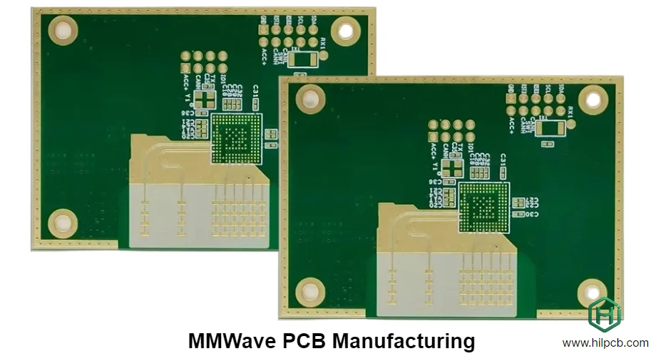
- A 5G phase shifter PCB must maintain RF path consistency, phase accuracy, and thermal stability across multiple antenna channels.
- The primary design reviews are RF path symmetry, insertion-loss budget, laminate selection, impedance control, control-line isolation, thermal behavior, and assembly repeatability.
- Beam steering performance depends on the complete RF chain, including transmission lines, connectors, grounding structures, materials, and assembly processes.
- Common failures occur when designers overlook path-length variation, dielectric changes, grounding transitions, temperature effects, or manufacturing tolerances.
- Successful prototype builds require early decisions on stackup, calibration access, measurement points, shielding, and production inspection methods.
A 5G phase shifter PCB provides the RF routing and control infrastructure that allows phased-array systems to adjust signal phase between antenna elements and electronically steer beams. The PCB design challenge is maintaining predictable phase response, controlled insertion loss, and stable operation across frequency and temperature while keeping the assembly manufacturable.
Contents
- What to review first on a 5G phase shifter PCB
- Key design and validation rule table
- Early engineering trade-off table
- How beam-steering accuracy affects layout choices
- How thermal drift and assembly details affect RF behavior
- What prototype and assembly teams should freeze before release
- FAQ
- Next steps
- References
- Author and review
What to review first on a 5G phase shifter PCB
A phase shifter does not determine beam steering performance by itself. The complete phased-array signal path controls the final result. Phase errors introduced by PCB routing, material variation, connectors, grounding, and assembly can reduce steering accuracy even when the phase shifter IC operates correctly.
The first design review should focus on:
- whether the phase shifter location matches the intended transmit or receive architecture
- whether RF paths between channels have consistent length, impedance, and reference structures
- whether the selected PCB material supports the required frequency range, loss target, and temperature environment
- whether digital control lines, bias networks, and power paths are separated from sensitive RF areas
- whether calibration points, test access, and measurement methods remain available after assembly and shielding
For mmWave and phased-array applications, engineers should align high-frequency PCB, Rogers PCB, and high-speed PCB requirements before finalizing the stackup.
A reliable design process starts with the RF path rather than the component placement alone. The PCB layout must preserve the electrical relationship between channels because beam steering relies on relative phase control.
Key design and validation rule table
| Rule / parameter | What to check first | Why it matters | How to verify | If ignored |
|---|---|---|---|---|
| Path symmetry | Compare RF routing geometry across all matched channels | Phase mismatch can reduce beam accuracy before calibration | Layout comparison and RF simulation review | Channel imbalance and unpredictable beam direction |
| Insertion-loss budget | Calculate loss across the complete RF chain | Phase shifter performance depends on surrounding components and interconnects | RF link budget review and VNA measurement plan | Reduced output power and inconsistent channels |
| Material stability | Select laminate based on dielectric performance, loss, and temperature behavior | Material variation changes impedance and phase response | Stackup review and laminate specification check | Increased calibration effort and phase drift |
| Control/RF isolation | Separate control signals, bias networks, and RF transmission paths | Digital noise and return-current paths can disturb RF performance | Floorplan review and grounding analysis | Noise coupling and unstable tuning |
| Thermal path | Analyze heat sources near phase-control devices | Temperature changes can affect insertion loss and phase accuracy | Thermal simulation and temperature testing | Steering errors and reduced repeatability |
| Test access | Define measurement access before mechanical packaging | RF debugging becomes difficult after shielding and assembly | DFT review and validation planning | Longer debug cycles and limited failure analysis |
Early engineering trade-off table
| Design choice | Usually stronger for | Main trade-off | What to confirm early |
|---|---|---|---|
| PTFE or low-loss RF laminate | Lower RF loss and improved high-frequency stability | Higher material cost and more complex fabrication | Operating frequency and loss requirements |
| Hybrid RF + FR-4 stackup | Cost balance with practical digital integration | Requires careful layer planning and controlled transitions | Which layers contain critical RF signals |
| Integrated phased-array submodule | Shorter RF paths and compact packaging | More concentrated thermal load and reduced service access | Calibration method and thermal extraction |
| Split RF and control boards | Improved RF isolation and easier partitioning | Additional connectors and interconnect losses | Mechanical constraints and connector performance |
| Additional shielding | Improved isolation in dense RF environments | Can affect thermal performance and inspection access | Shield design, testing method, and service requirements |
| Fine HDI routing | Dense control and bias escape routing | Higher manufacturing requirements | Package pitch, via structure, and yield impact |
How beam-steering accuracy affects layout choices
The phase shifter IC cannot compensate for every PCB-level inconsistency. Calibration can correct predictable channel differences, but excessive variation in the RF path reduces correction range and increases system complexity.
Three PCB layout decisions have the largest impact.
1. Keep matched RF channels electrically consistent
Channel matching requires more than equal trace length. Engineers must also control:
- bend geometry
- via transitions
- reference-plane continuity
- return-current paths
- connector interfaces
- local dielectric environment
A small difference between channels can create phase imbalance that affects beam direction and sidelobe performance.
The goal is not only matching measured length. The goal is creating the same electrical environment for every RF channel.
2. Design the PCB as part of the phased-array RF network
A phase shifter PCB connects with amplifiers, filters, mixers, antenna feed networks, and control circuits. Each transition influences RF performance.
Optimizing each component separately can create problems after integration. A transmission line that performs well in isolation may behave differently when connected to connectors, shields, packages, or adjacent circuits.
A Gerber viewer or PCB viewer review can help identify routing differences, layer transitions, and manufacturing risks before fabrication.
3. Plan calibration and measurement access during layout
Phased-array boards often become difficult to test after shields, connectors, and mechanical structures are installed.
The release package should define:
- RF probing locations
- calibration reference points
- shield removal requirements
- measurement sequence
- production inspection method
Designing measurement access after layout completion often requires expensive mechanical changes.
How thermal drift and assembly details affect RF behavior
Thermal stability is a critical requirement for phase shifter PCB designs because temperature changes can modify electrical characteristics. Dielectric properties, conductor dimensions, solder conditions, and component behavior can all influence phase response.
A board that performs correctly at room temperature may show measurable differences during operation if heat from nearby RF power devices or amplifiers changes the local environment.
Key engineering checks include:
- whether nearby PA devices, regulators, or bias circuits create thermal gradients near phase-control components
- whether copper distribution and laminate selection support stable RF performance across temperature changes
- whether solder volume, shield attachment, and component placement introduce channel-to-channel variation
- whether validation includes both RF measurement and temperature-based performance testing
For dense RF modules that combine routing, shielding, power distribution, and fine-pitch components, SMT assembly, turnkey assembly, and PCB prototype planning should be reviewed together.
Assembly variation can directly affect RF behavior. Connector alignment, solder joint consistency, and shield installation methods should be included in the RF validation plan rather than treated as separate manufacturing concerns.
What prototype and assembly teams should freeze before release
Prototype risk decreases when RF design requirements, thermal requirements, and manufacturing requirements are defined before fabrication.
A practical release checklist includes:
- Matched-channel RF routing approved
Freeze the RF geometry for comparable channels before final manufacturing release. - Material and stackup approved
Confirm laminate selection, dielectric properties, copper structure, and loss requirements. - Control and bias isolation reviewed
Verify that digital interfaces and power paths do not compromise RF performance. - Thermal analysis completed
Confirm heat sources and thermal paths near sensitive phase-control circuits. - Calibration and shielding strategy documented
Define measurement access and tuning procedures after assembly. - BOM review completed
Use a BOM viewer review to identify sourcing risks for RF components, connectors, shields, and specialized materials before procurement.
If RF routing, stackup, or assembly requirements are still changing, quick-turn PCB support can reduce iteration time before committing to volume manufacturing.
FAQ
Is the phase shifter IC the main factor controlling beam steering accuracy?
No. The phase shifter IC is only one part of the RF system. PCB routing consistency, stackup design, grounding, material stability, temperature behavior, and assembly quality all influence final beam steering performance.
Why is path symmetry important on a phase shifter PCB?
Beam steering depends on the relative phase relationship between channels. Differences in routing, transitions, or reference structures create channel mismatch and reduce steering predictability.
Does every phase shifter PCB require specialty RF laminate?
No. The entire PCB does not always require premium RF material. However, critical RF paths operating at higher frequencies typically require materials selected for controlled dielectric properties and low loss.
Why does assembly affect RF phase consistency?
Assembly changes the physical RF environment. Solder variation, connector placement, shielding methods, and manufacturing tolerances can change impedance, insertion loss, and phase response.
What should be finalized before a phase shifter PCB prototype build?
The most important items are the stackup, RF channel geometry, control routing strategy, thermal approach, calibration plan, and measurement access.
Next steps
For a 5G beamforming or phased-array module, the most effective first step is reviewing RF geometry, material selection, thermal behavior, and assembly requirements together before prototype release.
HILPCB can support phase shifter PCB development through:
- High-frequency PCB and Rogers PCB planning for controlled-loss RF routing
- High-speed PCB and HDI PCB support for dense control and bias circuitry
- SMT assembly and turnkey assembly coordination for shielded RF module manufacturing
- PCB prototype, quick-turn PCB, Gerber viewer, and PCB viewer support for early design verification
- Request a quote when your stackup, RF layout rules, and assembly requirements are prepared
References
- Analog Devices phased-array antenna patterns, beamwidth, and steering
- Analog Devices phased-array beam steering and phase shift
- Qorvo beamforming and phased-array resources
- Rogers RF and microwave materials
Author and review
Author: HILPCB Engineering Content Team
Reviewed by: HILPCB RF PCB and Beamforming Review Team
Last updated: 2026-04-09