
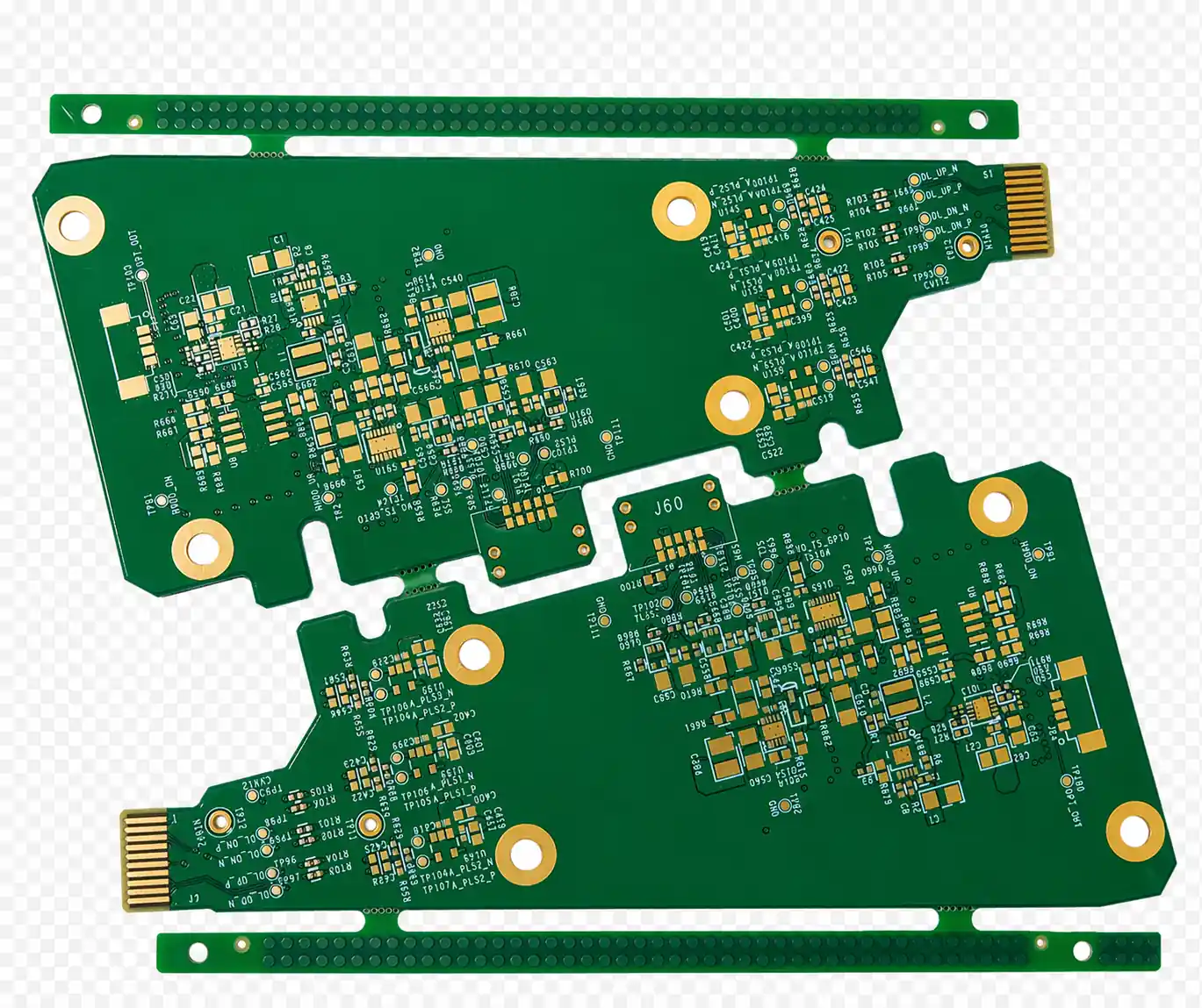
An 8 layer PCB is the architecture of choice when a design must deliver both high routing density and rigorous electromagnetic compatibility on the same board. With four signal layers and four plane layers, an 8 layer stack-up provides the shielding infrastructure necessary for mixed-signal designs—where analog sensor inputs, high-speed digital buses, switching power supplies, and RF wireless modules must coexist without mutual interference.
For projects balancing EMC pressure with routing density, teams often review multilayer PCB capability together with high-speed PCB constraints before locking the final layer arrangement.
But the decision to go to 8 layers is rarely driven by routing density alone. More often, it is driven by EMC certification pressure: a 6 layer board that fails radiated emissions testing needs the additional shielding that only a properly configured 8 layer stack-up can provide. Understanding when and how to make the transition—and which of the many possible 8 layer configurations best suits your design—is what this guide covers in detail.
The term "8 layer PCB" spans a wide range of constructions: standard FR-4 multilayer boards for industrial and consumer applications, high-Tg builds for automotive ECUs, hybrid stack-ups combining low-loss dielectrics with FR-4 for wireless devices, rigid-flex configurations for medical instruments, and HDI constructions with blind and buried vias for dense BGA routing. Each construction type shares the same layer count but requires different materials, process sequences, and design rules.
HILPCB Manufacturing Capability: Our 8 layer PCB fabrication delivers controlled impedance to ±8% (±5% available), supports blind and buried via structures, and provides full EMC-optimized stack-up engineering. Engineering teams from the UK, Switzerland, and Scandinavia rely on HILPCB for technically demanding 8 layer builds where EMC compliance must be achieved on the first production run—because a second board spin to fix emissions failures costs far more than getting the stack-up right from the start.
In This Guide
- When 6 Layers Are Not Enough: The Case for 8
- The Three Stack-Up Architectures Every Engineer Should Know
- Mixed-Signal Design: Analog and Digital on One Board
- Material Systems for 8 Layer PCBs
- 8 Layer PCBs for Wireless and RF Applications
- 8 Layer Rigid-Flex for Medical and Aerospace
- Via Architecture: From Through-Hole to Stacked Microvias
- Lamination Process and Thickness Control
- Impedance Control and Crosstalk Management
- Testing, Tolerances, and Quality Verification
- DFM Checklist for 8 Layer Designs
- Starting Your 8 Layer Project with HILPCB
When 6 Layers Are Not Enough: The Case for 8
The most common trigger for moving from 6 to 8 layers is not a shortage of routing space—it is a shortage of reference planes. A 6 layer board in the S-G-S-P-G-S configuration provides three signal layers and three reference planes. This works well for many designs, but it breaks down in three specific scenarios:
Scenario 1: Mixed-signal designs requiring analog/digital isolation. A data acquisition system with a high-resolution ADC needs separate analog and digital ground domains. On a 6 layer board, there is only one ground plane (or two, if you sacrifice a power plane). An 8 layer board can dedicate separate ground planes to analog and digital sections without splitting a single plane—which, contrary to common belief, usually makes noise coupling worse, not better.
Scenario 2: Complex power distribution with 4+ voltage rails. When a design requires 5V, 3.3V, 1.8V, and 1.2V rails—common in SoC-based designs—a 6 layer board must either split its single power plane into four islands or route some rails as power traces on signal layers. Both approaches degrade PDN performance. An 8 layer board can dedicate two full plane layers to power distribution, providing clean, low-impedance distribution for multiple voltage domains.
Scenario 3: EMC compliance for Class B (residential) certification. Products sold into residential markets must meet FCC Class B or CISPR 22 Class B emissions limits—which are 10dB more stringent than Class A (industrial) limits. The additional shielding planes in an 8 layer stack-up provide 6-12dB of additional emissions reduction compared to a 6 layer board with the same circuit, often making the difference between passing and failing pre-compliance testing.
The cost increase from 6 to 8 layers is typically 25-35% at the board level. For a product facing EMC certification, this increase is almost always less expensive than the alternative: adding shielding cans, ferrite beads, and common-mode chokes to a 6 layer board, then paying for multiple rounds of pre-compliance testing and board respins.
The Three Stack-Up Architectures Every Engineer Should Know
The layer arrangement of an 8 layer board determines its electromagnetic performance, routing capacity, and power delivery capability. While many variations exist, three architectures cover the vast majority of production designs.Architecture A: Optimal EMI Performance (Recommended Default)
| Layer | Function | Notes |
|---|---|---|
| L1 | Signal (Top) | Microstrip, referenced to L2 |
| L2 | Ground Plane | Continuous, unbroken |
| L3 | Signal (Inner 1) | Stripline, referenced to L2/L4 |
| L4 | Power Plane | Core voltage distribution |
| L5 | Ground Plane | Continuous, unbroken |
| L6 | Signal (Inner 2) | Stripline, referenced to L5/L7 |
| L7 | Power Plane | Secondary voltage rails |
| L8 | Signal (Bottom) | Microstrip, referenced to L7 |
This is the architecture HILPCB recommends as the starting point for any 8 layer design. Every signal layer is immediately adjacent to at least one continuous ground or power plane, ensuring that every trace has a well-defined return current path. The L2 and L5 ground planes provide vertical electromagnetic shielding, dividing the board into two isolated cavities that prevent coupling between the top-side and bottom-side circuits.
The L4-L5 power-ground pair—separated by thin dielectric (3-5mil)—functions as a distributed bypass capacitor with approximately 200-400pF/cm². This embedded capacitance provides high-frequency decoupling that discrete capacitors cannot match above 500MHz due to their parasitic lead inductance.
Architecture B: Maximum Routing Density
For designs where routing congestion is more critical than EMI performance, signal layers can be placed on L3, L4, L5, and L6, with ground/power planes on L1, L2, L7, and L8. This provides four inner signal layers fully shielded by the outer plane layers—forming a Faraday cage. The trade-off is that L4 and L5 share a reference boundary, which may create crosstalk between signals on these layers if they cross paths.
This architecture is useful for dense BGA fanout boards, test fixtures, and designs where external shielding (such as a metal enclosure) handles EMC compliance.
Architecture C: Dual Power Domain
Designs with complex power requirements—such as boards combining a processor (1.0V core, 1.8V I/O, 3.3V peripherals) with a power amplifier (5V or 12V rail)—benefit from three power plane layers. Architecture C assigns L2 as ground, L4 as primary power (processor rails), L5 as ground, and L7 as secondary power (amplifier/motor rails). Two inner signal layers (L3, L6) and two outer signal layers (L1, L8) provide adequate routing for most designs.
Mixed-Signal Design: Analog and Digital on One Board
8 layer boards frequently combine sensitive analog circuits (sensor amplifiers, precision ADCs, audio codecs) with noisy digital circuits (microprocessors, FPGAs, switching regulators). Proper domain isolation in the stack-up is essential for achieving the signal-to-noise ratio that the analog section requires.The Ground Plane Debate: Split or Unified?
The most common mistake in mixed-signal 8 layer design is splitting the ground plane between analog and digital domains. While this approach seems intuitive—separate grounds for separate circuits—it almost always makes noise coupling worse because return currents from signals crossing the split boundary are forced to flow around the gap, creating large current loops that radiate EMI. The high-impedance gap between the split sections acts as a slot antenna at frequencies above 100MHz, and the two ground sections develop a voltage difference that directly adds noise to the analog signals.
The correct approach for most designs: Use continuous, unbroken ground planes on L2 and L5. Rely on physical placement to separate analog and digital components into distinct board areas. Route analog signals exclusively on one layer (L3) and digital signals on another (L6). Place the ADC/DAC at the boundary between domains, with its analog ground pins connecting to the ground plane in the analog region and its digital ground pins connecting in the digital region.
Power Supply Isolation
Where true voltage domain isolation is required—for example, separating a sensitive analog reference voltage from the switching regulator output—dedicate one power plane layer (L4) to digital power and another (L7) to analog power. Each domain receives its own set of bypass capacitors and a clean connection to the unified ground plane.
Guard Traces and Via Fencing
On signal layers carrying sensitive analog signals, guard traces connected to ground can be routed alongside critical traces (reference voltage lines, low-level sensor inputs). These guard traces should be stitched to the ground plane with vias spaced at λ/20 of the highest frequency of concern. At 100MHz, this means vias every 15mm; at 1GHz, every 1.5mm.
Material Systems for 8 Layer PCBs
The total board thickness for an 8 layer PCB typically ranges from 1.2mm to 2.0mm, with 1.6mm being the standard default. Material selection affects electrical performance, thermal reliability, and cost.Standard and High-Tg FR-4
At 8 layers, high-Tg FR-4 (Tg ≥170°C) is the recommended default for professional designs. The additional thermal stability improves via reliability during lead-free assembly and ensures dimensional stability through multiple reflow cycles. Materials like ITEQ IT-180A (Tg 175°C) and Isola 370HR (Tg 180°C) are industry standards for 8 layer boards destined for industrial, medical, and automotive applications.
Standard FR-4 (Tg 130-150°C) is adequate for consumer designs with no more than 2 reflow cycles and operating below 100°C.
Low-Loss Laminates for Higher Frequencies
Designs operating at 2-6GHz—WiFi 6E access points, Bluetooth 5.2 modules, cellular IoT gateways—may require low-loss dielectric materials on specific layers. A hybrid stack-up uses Panasonic Megtron 4 (Dk 3.8, Df 0.005 at 10GHz) for the signal layers carrying RF or high-speed traces, with standard FR-4 for the remaining core layers to control cost.
The key consideration for hybrid 8 layer stacks is CTE matching between material systems. Megtron 4 and high-Tg FR-4 have similar CTE values (both glass-reinforced, 14-16 ppm/°C in X-Y) and can be co-laminated safely. More exotic materials like PTFE/Teflon have higher CTE mismatch (24 ppm/°C) and are typically limited to 2 layers within an 8 layer hybrid stack.
Halogen-Free Options
For products requiring environmental compliance (EU RoHS evolution, IEC 61249-2-21), halogen-free 8 layer boards use materials like Shengyi S1150G with modified processing parameters (5-10% higher lamination pressure).
8 Layer PCBs for Wireless and RF Applications
Wireless devices increasingly require 8 layers to accommodate the routing density of modern SoCs while providing proper RF signal routing. A [WiFi 6E router](/blog/telecom-pcb), for example, needs antenna feeds, RF filtering, power amplifier bias networks, digital processing, memory interfaces, and Ethernet—all on a single board.A typical 8 layer RF/digital hybrid places the RF signal layer (L1) on Rogers 4350B or Megtron 4 for antenna feed networks and matching circuits, with the remaining layers on cost-effective FR-4. The Rogers-to-FR-4 boundary uses Rogers 4450F bondply or FR-4 prepreg for bonding.
When signals transition between the RF layer and digital layers, via transitions create impedance discontinuities. Minimize these by surrounding every signal via with at least 4 ground vias placed within one via diameter.
8 Layer Rigid-Flex for Medical and Aerospace
While less common than at lower layer counts, 8 layer [rigid-flex constructions](/products/rigid-flex-pcb/) serve critical applications where connector elimination directly improves system reliability.A typical 8R-2F configuration runs 2 flex layers through both rigid and flex zones, with 6 additional rigid layers in rigid sections only. Manufacturing requires adhesiveless polyimide (Kapton or UPILEX, 25-50μm), rolled annealed copper for fatigue resistance, coverlay film in flex zones, controlled-depth Z-routing with ±4mil accuracy, and no-flow prepreg at transition zones.
Minimum bend radius: 0.9mm static (6× thickness) and 3mm dynamic (20× thickness) for a 2-layer flex section.
 Optimized 8 layer stack-up architecture showing four signal layers each paired with a dedicated reference plane. This configuration provides the electromagnetic shielding that industrial data acquisition systems and medical monitoring equipment require to pass EMC certification—a key reason why hardware engineers across Western Europe and North America consistently select 8 layers for mixed-signal designs that must meet CISPR 22 Class B emissions limits.
Via Architecture: From Through-Hole to Stacked Microvias
### Through-Hole ViasStandard through-hole vias penetrate all 8 layers. For a 1.6mm board, the maximum aspect ratio of 10:1 permits minimum finished holes of 0.15mm. Sufficient for most designs using components with pitch ≥0.65mm.
Blind Vias (L1-L2 and L7-L8)
Blind vias connecting the outer layer to the adjacent plane require sequential lamination. Laser-drilled blind vias can be as small as 0.1mm diameter, enabling signal escape from fine-pitch BGA packages with 0.5mm pitch. Adding blind vias increases cost by approximately 15-25%.
Buried Vias and Stacked Microvias
Buried vias connect only inner layers and are formed within inner cores before final lamination, adding 20-40% cost. Stacked microvias (blind via on buried via) provide maximum density for 0.4-0.5mm pitch BGA packages.
Lamination Process and Thickness Control
An 8 layer board uses three double-sided cores and two prepreg bond layers. For HDI designs, sequential lamination adds a second press cycle. Standard dielectric thickness tolerance is ±10%, translating to ±5-8% impedance variation.8 layer boards are susceptible to warpage if the stack-up is asymmetric—maintain copper density balance between opposing layer pairs (L1/L8, L2/L7, L3/L6, L4/L5). The IPC limit is 0.75% of diagonal dimension.
Impedance Control and Crosstalk Management
### Common Impedance Targets| Interface | Impedance | Topology |
|---|---|---|
| USB 2.0/3.x | 90Ω differential | Stripline preferred for 3.x |
| Gigabit Ethernet | 100Ω differential | Either |
| PCIe Gen 1-3 | 85Ω differential | Stripline |
| DDR3/DDR4 DQ | 40-60Ω single-ended | Either |
| HDMI / LVDS | 100Ω differential | Either |
| General digital | 50Ω single-ended | Either |
Crosstalk Management
Intra-layer crosstalk: maintain spacing per the "3W rule" (3× trace width) for 70% isolation. Inter-layer crosstalk between signals on different layers is managed by dielectric thickness between signal layers. Orthogonal routing (horizontal on one layer, vertical on the adjacent) reduces inter-layer coupling.
Testing, Tolerances, and Quality Verification
| Parameter | Standard | Advanced | | :--- | :--- | :--- | | Board thickness | ±10% | ±8% | | Impedance control | ±10% | ±8% (±5% available) | | Layer registration | ±3mil (75μm) | ±2mil (50μm) | | Min. trace/space | 3.5/3.5mil | 3/3mil |All boards undergo 100% electrical testing. Impedance verified by TDR on 3-5 coupon structures per panel. Cross-section analysis verifies via plating (min. 25μm for IPC Class 3), dielectric thickness, and registration accuracy. For high-speed designs requiring insertion loss verification, VNA measurements confirm channel performance.
DFM Checklist for 8 Layer Designs
Before releasing your 8 layer design:- Every signal layer has an adjacent continuous reference plane
- Power plane splits do not cross critical signal routing paths
- Stack-up is symmetric for warpage prevention; copper balance within ±20%
- High-speed differential pairs routed on stripline layers for maximum shielding
- Via stubs acceptable for operating frequency (consider back-drilling above 5GHz)
- Decoupling capacitors within 3mm of IC power pins with dedicated vias
- Minimum trace/space achievable by target process
- Solder mask dams between fine-pitch pads ≥3mil wide
Starting Your 8 Layer Project with HILPCB
HILPCB delivers 8 layer PCB fabrication across all construction types with integrated [SMT assembly](/products/smt-assembly/) for complete turnkey production.Stack-Up Engineering: Free DFM review with impedance simulation using Polar SI tools—optimal layer arrangement for your EMI, impedance, and routing requirements.
Material Flexibility: Standard FR-4, high-Tg, low-loss (Megtron 4/6), Rogers 4350B, halogen-free, and polyimide rigid-flex—all from stock.
HDI and Fine Features: Blind vias to 0.1mm, buried vias, via-in-pad, 3/3mil trace/space, sequential lamination.
Quality: 100% electrical testing, TDR impedance verification, cross-section analysis, IPC-A-600 Class 2/3. ISO 9001, IATF 16949, ISO 13485 certifications.
Prototype to Production: 48-hour express prototypes scaling to high-volume production with SPC monitoring. Customers across the US, Canada, Germany, UK, France, Scandinavia, and Australia receive dedicated engineering support with same-day DFM feedback.
Upload your Gerber files for a free 8 layer stack-up review and quotation →