
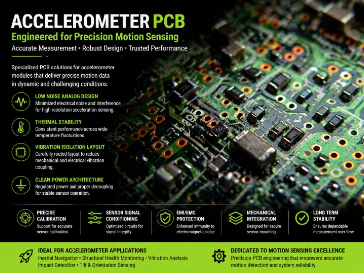
Accelerometers measure linear acceleration — the rate of change of velocity along one or more axes. The global accelerometer market reached $3.16 billion in 2024 and is projected to exceed $5.2 billion by 2031, driven by automotive ADAS, industrial condition monitoring, and defense inertial navigation applications. Every accelerometer is only as good as the PCB it's mounted on — board-level noise, resonance, and mounting stress directly determine whether the sensor achieves its rated specification or delivers degraded data.
HILPCB serves accelerometer PCB programs ranging from 2-layer consumer IoT boards at $0.50 per unit through 16-layer navigation-grade IMU assemblies exceeding $800 per board — with over 200 sensor PCB programs delivered to OEMs across North America, Europe, and Asia-Pacific since 2019. Our IPC-6012 Class 3 fabrication and SMT assembly with controlled reflow profiles address the unique sensitivity of MEMS sensors to soldering-induced stress.
In This Guide
- MEMS Accelerometer PCB Interface and Mounting
- Piezoelectric Sensor Signal Conditioning
- High-G Shock Measurement Board Design
- Industrial Vibration Monitoring and Wireless IoT Nodes
- Environmental Compliance and Production Testing
- HILPCB Accelerometer PCB Capabilities
MEMS Accelerometer PCB Interface and Mounting
MEMS accelerometers measure the acceleration of the PCB pad they are soldered to — not the overall system. Any resonance or compliance between the mounting point and the structure being measured corrupts the measurement before electronics can process it. This fundamental fact drives every design decision from board stiffness to sensor placement to panelization strategy.Digital MEMS sensors from Analog Devices (ADXL355, ±3.6 μg/√Hz noise density), Bosch (BMA400), and STMicroelectronics (LIS2DW12) provide SPI or I²C output. The PCB interface appears simple — decoupling and a bus connection — but achieving sensor-rated performance demands that the sensor be placed near a board mounting screw, not at the center of an unsupported span where board resonance amplifies some frequencies and attenuates others.
For tactical and navigation-grade MEMS (Honeywell HG4930, Northrop Grumman LN-200A), the PCB provides an external analog signal chain: instrumentation amplifier matched to the ADC range, 4th-order Butterworth anti-aliasing filter (100–500 Hz), and 24-bit sigma-delta ADC with <1 μVrms input noise. Layout requires guard traces around analog inputs, thermally symmetric copper on both sides of differential pairs, and stripline shielding on multilayer boards — the same precision analog discipline used in laboratory instrumentation.
| Technology | Range | Bandwidth | Resolution | Typical Application |
|---|---|---|---|---|
| Consumer MEMS | ±2–16 G | 0–1 kHz | 1 mG | Smartphones, wearables |
| Tactical MEMS | ±10–50 G | 0–500 Hz | 10 μG | UAV navigation, munitions |
| Piezoelectric | ±50–10,000 G | 1 Hz–30 kHz | 0.1 mG | Machine vibration monitoring |
| Piezoresistive | ±100–200,000 G | 0–100 kHz | 1 G | Automotive crash testing |
| Capacitive servo | ±1–60 G | 0–300 Hz | 0.1 μG | Seismic, inertial navigation |
Soldering stress during SMT assembly can bias MEMS output by several degrees per second through differential thermal expansion between sensor package and PCB substrate. HILPCB addresses this with manufacturer-specified reflow profiles, laser or routed depaneling (never V-score break), and 24–72 hour stress relaxation before factory calibration.
Piezoelectric Sensor Signal Conditioning
Piezoelectric accelerometers dominate vibration monitoring applications in automotive manufacturing plants across Germany (BMW Dingolfing, Mercedes Sindelfingen, Continental), rotating machinery in oil refineries across the US Gulf Coast and North Sea platforms, and structural health monitoring for bridges and aircraft throughout the United Kingdom, Scandinavia, and Canada. The global vibration monitoring market reached $1.8 billion in 2023, growing at 6.5% CAGR driven by Industry 4.0 adoption.Two interface modes create fundamentally different PCB challenges. Charge-mode accelerometers output electrical charge proportional to acceleration — the PCB requires a charge amplifier with >10 GΩ input impedance, demanding guard rings, PTFE standoff insulators, and high-Tg FR-4 cleaned to remove ionic contamination. Board contamination (flux residue, fingerprints) drops surface resistance below 10 GΩ within hours, causing signal drift that manifests as low-frequency measurement errors.
IEPE (Integrated Electronics Piezoelectric) sensors — the industry standard for industrial vibration — include built-in charge amplifiers outputting voltage on a 2–20 mA constant-current supply. The PCB interface simplifies to current source, AC coupling capacitor, and ADC input. HILPCB assembles multi-channel IEPE acquisition boards with up to 32 simultaneous channels, each with dedicated 24-bit ADC at 51.2 kSPS — no multiplexing, which introduces inter-channel phase error that corrupts machine diagnostics.
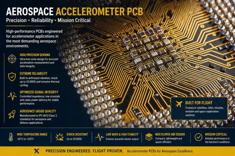 Multi-channel vibration monitoring PCB manufactured by HILPCB with 16 simultaneous IEPE input channels for structural health monitoring applications across US and European infrastructure programs.
High-G Shock Measurement Board Design
Crash testing at BMW (Munich), NHTSA (Washington), and Euro NCAP (Brussels), ballistic impact recording for defense programs, and pyrotechnic shock measurement for launch vehicles all require PCBs that survive 10,000–200,000 G while capturing data from a single unrepeatable event.At 20,000 G, a standard 0805 capacitor (mass: 0.1 g) experiences 20 N of force — enough to shear the solder joint. Every component on a high-G board becomes a structural element whose mass directly determines whether it survives. HILPCB's high-G board construction uses:
- Miniaturized Components: 0201 or 01005 passives exclusively — 10× less mass means 10× less force at any G-level. Our pick-and-place systems achieve ±25 μm placement accuracy on 01005 parts.
- Heavy Copper Stiffening: ≥2.0 mm board thickness with 2 oz internal copper layers providing rigidity that pushes board resonance frequencies above the measurement bandwidth.
- Component Reinforcement: Underfill on all BGAs, epoxy staking on tall components, through-hole mounting for the primary accelerometer connector.
- Autonomous Data Capture: Continuous circular buffer recording at 500 kSPS–2 MSPS with pre-trigger capture and ruggedized flash storage surviving the shock independently — because the cable to the recording system may not survive.
Industrial Vibration Monitoring and Wireless IoT Nodes
The industrial vibration monitoring market is shifting from permanently wired systems to battery-powered wireless nodes — reducing installation cost from $3,000–5,000 per measurement point (wired) to $500–1,000 (wireless). This shift creates new PCB challenges around power management, on-board signal processing, and wireless communication.At HILPCB, we fabricate both multi-channel wired acquisition boards and compact wireless sensor nodes for Industry 4.0 condition monitoring deployments.
Industrial IoT Sensor Node Design
- Ultra-Low Power: Target 3–5 year battery life through duty-cycled measurement (1 second every 10 minutes at <5 μA quiescent current). HILPCB's HDI construction enables compact 25×30 mm node boards with integrated antenna.
- On-Board FFT Processing: Transmitting only spectral data reduces radio-on time by 90%+ versus raw waveform streaming — extending battery life while providing the frequency-domain information maintenance engineers need.
- Wireless Protocols: BLE 5.0 for short-range (factory floor), LoRaWAN for facility-wide coverage — with high-frequency PCB antenna structures integrated on the sensor board.
- Environmental Protection: Conformal coating per IPC-CC-830 — acrylic for general industrial, silicone for high-temperature machinery (up to 200°C near furnaces). ATEX/IECEx certification support for oil and gas installations.
Wired Acquisition System Design
Multi-channel acquisition boards serving predictive maintenance programs require simultaneous sampling across 4–32 channels with matched analog paths (±0.1% resistors, ±1% capacitors) ensuring <0.5° inter-channel phase matching. Data interfaces include 4–20 mA for legacy PLCs, Modbus RTU/TCP, and OPC UA for Industry 4.0 integration.
Environmental Compliance and Production Testing
Accelerometer PCB qualification varies dramatically by application sector. Automotive crash sensors require IATF 16949-certified manufacturing meeting tier-one supplier quality systems — HILPCB's automotive-qualified production line supports OEMs and Tier 1 suppliers including programs for Continental (Hanover), ZF (Friedrichshafen), and Aptiv (Dublin/Shanghai).Aviation accelerometer PCBs comply with DO-160G environmental testing and DO-254 hardware assurance for DAL-A/B applications. Defense IMU boards meet MIL-STD-810H vibration (5–2000 Hz, 3–5G RMS) and thermal cycling (-55°C to +85°C, 1000+ cycles per IPC-9701).
MEMS sensors are ESD-sensitive — HILPCB enforces full ESD-safe handling with HBM protection >2 kV on all sensor lines. Our production testing protocol includes 100% electrical verification, functional test with calibrated reference acceleration, and mounting stress verification through pre/post-assembly bias comparison.
HILPCB Accelerometer PCB Capabilities
HILPCB has delivered over 200 accelerometer and vibration sensor PCB programs since 2019, serving OEMs across the United States (defense IMU, automotive), Germany (automotive tier-1, industrial), France (aerospace navigation), the United Kingdom (structural health monitoring), Canada (oil and gas), and Scandinavia (marine and offshore vibration).Our platform delivers consumer IoT sensor boards on 2–4 layer FR-4 at volumes exceeding 50,000 units per year, industrial vibration monitoring on 6–8 layer controlled-impedance constructions, high-G shock boards with heavy copper stiffening and 01005 component capability, and navigation-grade IMU assemblies on 10–16 layer boards with rigid-flex for multi-axis sensor configurations.
From prototype through volume production, our DFM review addresses board stiffness for measurement accuracy, channel matching for multi-sensor arrays, and reflow profile optimization for stress-sensitive MEMS assemblies. Typical lead times: 5–7 days for prototype, 2–3 weeks for production.
Accelerometer PCB FAQ
How does board stiffness affect accelerometer performance?
MEMS accelerometers measure the acceleration of the PCB they are mounted on. If the PCB is not sufficiently stiff, board resonance can amplify or attenuate specific frequencies, corrupting the measurement data. Using thicker boards (e.g., 2.0 mm) and heavy copper layers helps push resonance frequencies above the measurement bandwidth.
Why are guard traces required for piezoelectric sensor PCBs?
Charge-mode piezoelectric accelerometers output a very small electrical charge. The PCB requires a charge amplifier with extremely high input impedance (>10 GΩ). Guard traces prevent leakage currents from contaminating the signal, ensuring accurate low-frequency measurements without drift.
How do you prevent SMT assembly from damaging MEMS sensors?
MEMS sensors are highly sensitive to thermal and mechanical stress during soldering, which can bias their output. We use manufacturer-specified controlled reflow profiles, laser or routed depaneling instead of V-scoring, and enforce a 24-72 hour stress relaxation period before factory calibration.