
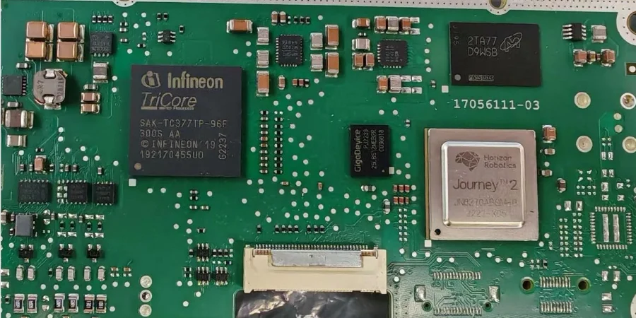
An ADAS camera-module PCB should be released from its actual interface, channel, power, thermal, mechanical and evidence requirements. Freeze those inputs before choosing a layer build or asking for a production quote. The PCB can carry and connect the camera electronics; it does not, by itself, qualify the camera module, vehicle, perception function or functional-safety case.
This guide helps three groups make the handoff explicit:
- Designer/EE: select the local image-sensor/ISP path or the automotive SerDes path, then protect signal and power margins through stack-up and layout review.
- Quality/NPI: assign each acceptance record to the bare board, PCBA, camera module or vehicle program, with revision and lot traceability.
- Procurement: compare suppliers using the same construction, inspection, test and deliverable assumptions instead of a board-only price.
The short answer: choose the camera-board path from the link and release evidence
Start with the selected image sensor, ISP/SoC, serializer/deserializer and connector data sheets. A local MIPI CSI-2 path keeps the high-speed camera interface on the module or nearby board. An automotive SerDes path adds a device-specific channel through a connector, cable or harness. The two paths can require different reference planes, transitions, AC-coupling, power filtering, EMC controls and validation fixtures.
For either path, the release package should freeze:
- The interface part numbers, topology, lane mapping, clocking and allowed channel model.
- The stack-up, material family, copper and pressed-dielectric assumptions, impedance nets and return-plane continuity.
- HDI, microvia, backdrill, connector launch, keep-out and mechanical flatness requirements.
- Sensor/processor power rails, startup states, thermal path, enclosure and contamination constraints.
- Inspection, electrical, programming and functional evidence, including who supplies each fixture, limit and report.
Use high-speed PCB manufacturing, HDI PCB capabilities, and SMT assembly as starting points for a quote. The actual construction, coverage and records remain quotation-defined.
MIPI CSI-2 or automotive SerDes: what must be frozen?
MIPI CSI-2 is a board-level camera interface specification family. It does not select a universal trace geometry or establish a completed module's image performance. A SerDes implementation is even more dependent on the selected vendor's data sheet and layout guide. Do not copy a generic impedance, length, skew or loss value into a release drawing.
| Board path | Freeze before layout | Board-level controls | Evidence to request | Primary owner |
|---|---|---|---|---|
| Local MIPI CSI-2 | Sensor/ISP part numbers, lane mode, clocking, connector or flex details, device layout rules | Continuous reference plane, controlled pair geometry, short transitions, decoupling and test access | Released stack-up and net table; coupon/TDR record when specified; powered bring-up result | Customer/project team with component vendor rules |
| Automotive SerDes | Serializer/deserializer pair, cable/connector topology, channel budget, coupling and power-over-coax rules | Connector launch, pair symmetry, return path, protection/filter placement and via transition review | Vendor-guide review; quoted channel or fixture test if required; link diagnostics | Customer/project team and component vendor |
| Shared power and clock | Rail sequence, load transients, reset behavior, reference-clock source and monitoring | PDN placement, current-loop area, ground strategy, clock isolation and accessible probes | Quoted electrical or functional record against customer limits | Customer defines behavior; manufacturer records agreed tests |
The component vendor owns device limits and recommended layout conditions. The customer or project team owns system topology and acceptance criteria. The PCB manufacturer can review manufacturability and build to the released requirements after engineering review.
How should stack-up, return paths and HDI transitions be reviewed?
Treat the stack-up as an electrical and manufacturing contract, not a layer-count shortcut. Record the laminate family, pressed dielectric targets, copper profile, solder-mask assumptions, controlled nets, impedance method and substitution rules. A low-loss material is justified only when the selected channel model and fabrication correlation require it; the camera application name alone is not a material specification.
Return-path checks
- Keep each fast differential pair adjacent to a continuous reference plane through the useful route.
- Do not cross plane voids, split boundaries or connector keep-outs without an intentional return-path transition.
- Place power-entry filtering and local decoupling from the rail-current loop, not only by schematic proximity.
- Review the sensor, processor, converter and SerDes return currents together so a “quiet” camera area does not force a noisy detour.
HDI and via-transition checks
- Use microvias, blind/buried vias or VIPPO only where package escape, density or via-stub risk justifies the additional process and inspection plan.
- Define the build-up sequence, via-in-pad filling, aspect-ratio assumptions and backdrill locations in the released drawing.
- Check connector launches, BGA escapes, plane changes and test pads as one channel rather than isolated footprints.
- Ask for stack-up feasibility and coupon requirements before freezing a substitute material or sequential-lamination route.
The HDI PCB page and high-speed PCB page describe review topics. They are not a promise that every layer build, material combination or link test is included in every order.
Power, thermal, mechanical and EMC risks belong in the same review
An image sensor and ISP/SoC can be electrically sensitive while the enclosure creates a difficult thermal and mechanical boundary. Review these interactions before prototype release:
| Risk area | Design question | Useful release evidence |
|---|---|---|
| Power integrity | Do startup, steady load and processor/sensor transients stay within the customer rail limits? | PDN assumptions, probe points, quoted powered-board record and limit sheet |
| Thermal path | Does the component pad, copper, thermal via, shield or enclosure path match the allowed temperature profile? | Thermal model or measurement owned by the project; assembly void/connection evidence when specified |
| Mechanical fit | Are outline, connector position, fasteners, flatness, flex forming and optical-window keep-outs controlled? | Released mechanical drawing, first-article dimensions and assembly inspection record |
| EMC risk | Are return paths, filters, shielding and cable exits arranged to reduce coupling at the module boundary? | Layout review and customer or qualified-lab EMC plan; no automatic vehicle pass claim |
| Contamination | Could residue, particles, coating or handling affect the lens, connector or high-impedance node? | Agreed handling/cleanliness method and inspection record, if required by the program |
The PCB manufacturer can control the agreed construction and assembly process. The customer or module integrator owns enclosure, optical alignment, vehicle harness and system-level EMC/environmental validation.
Camera-module release matrix
Use this matrix as a release gate. Replace “when specified” with the customer's method, revision, sample plan and acceptance limit before production approval.
| Requirement | Board/assembly control | Evidence to request | Owner |
|---|---|---|---|
| Interface channel meets the selected device rules | Stack-up, pair geometry, plane continuity, connector/via review | Released net/impedance table; vendor-guide review; quoted coupon or channel record | Customer/project team and component vendor define; manufacturer reviews/builds |
| Bare board matches the released construction | Material, copper, drilling, plating, finish and electrical-test route | Fabrication drawing, material/lot record, bare-board electrical test and dimensional record | PCB manufacturer within quoted scope |
| HDI or fine-pitch escape is manufacturable | Build-up sequence, filled vias, pad design, inspection access and panel plan | Feasibility review, cross-section/microsection when quoted, first-article dimensions | PCB manufacturer; customer approves design tradeoffs |
| Soldered joints and hidden packages are acceptable | Stencil, placement, reflow profile and selected SPI/AOI/X-ray coverage | Programmed inspection records, profile, selected images or analysis, acceptance basis | Assembler within quoted scope; customer defines critical locations |
| Power-up and programming are repeatable | Test pads, firmware/configuration revision, fixture access and limits | ICT/flying-probe/boundary-scan or functional record when quoted | Customer supplies firmware, fixture and behavior limits; assembler executes agreed route |
| Camera image or link function is validated | Accessible connectors, loopback or module fixture defined in the test plan | Functional result format and sample plan | Customer/module integrator; third party if required |
| Environmental and EMC requirements are closed | Board construction, coating, shielding and mounting features support the plan | Customer or qualified-lab report to the named method and revision | Customer/project authority or qualified lab |
| Traceability and change control are closed | Revision, lot, component batch, rework and nonconformance linkage | First-article, CoC, inspection/test records and change log as quoted | Manufacturer supplies agreed records; customer controls release |
This matrix deliberately separates a manufacturing record from product qualification. A selected X-ray image, for example, can document a hidden-joint inspection location; it does not prove module lifetime or vehicle performance.
What evidence should exist at each NPI gate?
Use the project terminology (EVT/DVT/PVT or equivalent), but keep the evidence layers distinct:
- Engineering build: confirm interface bring-up, power sequencing, test access, DFM/DFA findings, thermal assumptions and mechanical fit.
- Design validation: verify the representative camera module against customer electrical, optical, mechanical, environmental, EMC and diagnostic requirements.
- Production validation: confirm the intended material route, fixtures, programming, inspection coverage, traceability, packaging, reaction plan and change controls.
- Release: approve the complete evidence package and identify requalification triggers such as stack-up, material, component, supplier, stencil, paste, reflow, coating, fixture or software changes.
AOI covers accessible features; it is not a substitute for every hidden-joint or functional check. X-ray/AXI, cross-section, electrical test, programming and functional test each answer a different question. Coverage, limits and report retention must be stated in the quotation and customer control plan.
Who owns standards, qualification and test decisions?
Standards provide requirements or methods; they do not automatically certify a PCB or PCBA. The applicable edition and acceptance class must be named in the RFQ.
- PCB manufacturer: confirms feasible fabrication and assembly routes, performs the quoted controls, and supplies the quoted records for the released construction.
- Customer/project team: owns system requirements, interface selection, firmware, fixtures, acceptance limits, product risk analysis and release approval.
- Component vendor: owns device data sheets, package guidance, operating limits and change notifications for its parts.
- Qualified third-party laboratory: performs independent environmental or EMC work when the customer requires a laboratory method or accreditation outside the manufacturer's quoted scope.
ISO 26262 is a vehicle functional-safety framework, not a statement that a bare PCB is “ASIL compliant.” AEC-Q component qualification does not qualify a populated board or camera module. ISO 16750, CISPR 25, IPC and MIPI requirements likewise apply according to the named part, edition, product level and test plan. Confirm those boundaries before using a standard in a purchase order or release record.
Camera PCB RFQ and release checklist
Submit enough information for the supplier to quote the real construction and evidence plan:
Design package
- Gerber or ODB++, NC drill, netlist, fabrication drawing, board outline, stack-up and revision identifiers.
- Controlled-impedance nets, target method/tolerance, coupon preference, backdrill/HDI details and material/substitution rules.
- Image-sensor, ISP/SoC, serializer/deserializer and connector part numbers with current data sheets and layout guides.
- Interface topology, lane mapping, clocking, channel/cable information, power-rail table and test points.
Assembly and mechanical package
- BOM with MPNs, AVL/approved alternates, placement data, assembly drawing, polarity/DNI rules and package handling requirements.
- Enclosure, connector, fastener, flatness, flex-forming, coating/potting, thermal and contamination constraints.
- Prototype, pilot and production quantities, sourcing ownership and required revision/change-control process.
Evidence request
- State which of stack-up review, impedance coupon/TDR, bare-board electrical test, first-article dimensions, SPI/AOI, selected X-ray/AXI, cross-section, programming, ICT/flying probe or functional test is required.
- Provide the test procedure, firmware, fixture/access, limits, sample plan, report format and retention rule for customer-defined tests.
- Request the quotation's inclusions, exclusions, process route, material assumptions, inspection coverage, traceability depth and deliverable list.
What can HILPCB support?
HILPCB can review the released fabrication and assembly package, discuss stack-up and HDI feasibility, coordinate controlled-impedance requirements, identify DFM risks, and quote agreed fabrication, SMT assembly, inspection and electrical or functional records. Exact equipment, coverage, test method, sample plan and report delivery are confirmed per quotation; a capability page is not a substitute for that project review.
Use the full Request a Quote form and include the camera-interface data, stack-up, BOM, mechanical constraints and evidence request above. The quote should make open questions and exclusions visible before prototype approval.
HILPCB does not replace the customer's camera/module design authority, component qualification, optical calibration, vehicle integration, functional-safety process, or qualified-lab environmental and EMC approval. The project team remains responsible for deciding whether the complete camera module and vehicle function are ready for release.
Frequently asked questions
Does every ADAS camera PCB need a low-loss laminate?
No. Select the material from the chosen interface's electrical model, route length, loss and phase budget, thermal behavior, copper construction and fabrication correlation. The camera application name alone is not enough.
Is MIPI CSI-2 the same as an automotive SerDes camera link?
No. MIPI CSI-2 commonly describes a local camera data interface, while an automotive SerDes path adds a selected serializer/deserializer, connector or cable channel and vendor-specific layout rules. Freeze the exact parts and topology before setting board rules.
Does a controlled-impedance coupon prove the complete camera link?
No. A coupon can document a quoted fabrication method for the board construction. Populated connectors, packages, cables, fixtures and the selected SerDes or MIPI device still require the project-defined channel or functional evidence.
Does AEC-Q or ISO 26262 qualify the PCB?
No. Component qualification and vehicle functional-safety work have different scopes. The customer or product authority must allocate requirements and approve module/system evidence; the manufacturer supplies only the agreed manufacturing records.
Which camera-board tests should be 100%?
There is no universal list. Define coverage by failure risk and detection purpose. Bare-board electrical test, AOI, selected X-ray/AXI, programming and functional checks detect different conditions, so the unit, feature, method and acceptance rule must be named.
Build a traceable camera-module release case
The efficient handoff is a linked record: interface requirements drive the stack-up, design risks drive process controls, and quoted inspections and tests produce evidence tied to a revision and lot. Give HILPCB the released files and the ownership boundaries so the Request a Quote response can state what is feasible, what is included, and what still belongs to the project team or a qualified laboratory.
Reference basis: MIPI Alliance, Camera Serial Interface 2 (MIPI CSI-2) overview; Texas Instruments, Automotive 2-MP Camera Module Reference Design With MIPI CSI-2, PMIC, FPD-Link III and POC (TIDUEB1); the selected component vendors' current data sheets and layout guides; and the customer-named ISO/IPC/EMC revisions.