
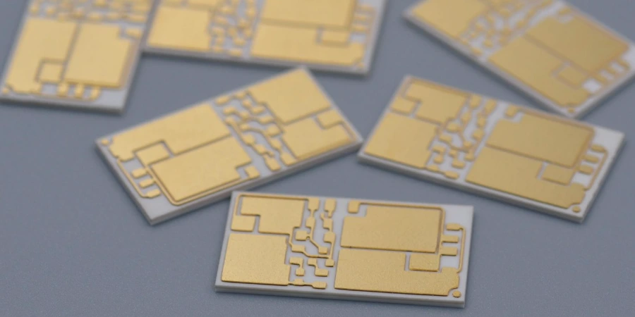
Al2O3 ceramic PCBs are widely used when FR-4 can no longer handle the heat, voltage or reliability requirements of modern power and RF electronics. This guide explains how alumina substrates work, how they compare with other materials, and what thick-film, thin-film and DBC processes mean in practice. It is written for design engineers and sourcing teams who need to improve thermal performance, increase lifetime and select a capable ceramic PCB manufacturer with confidence.
1. Why Choose Al2O3 Ceramic PCBs? Key Advantages over FR-4
For power electronics, RF/microwave, and harsh-environment systems, conventional organic printed circuit boards (FR-4, polyimide, etc.) are reaching their limits. Al2O3 (alumina) ceramic PCBs offer a unique combination of thermal, electrical, and mechanical properties that make them a preferred platform for high-power, high-voltage, and high-temperature applications.
For engineers and sourcing teams looking for high-reliability solutions, understanding the value of Al2O3 is essential. Compared with AlN (aluminum nitride), Al2O3 substrates offer balanced performance, mature processes, and significantly better cost efficiency—often the ideal entry point into the ceramic PCB world.
1.1 Four Critical Technical Advantages of Al2O3
| Advantage Area | Al2O3 Performance Range | Practical Benefit in Electronic Packaging |
|---|---|---|
| Thermal performance | Thermal conductivity K ≈ 20–30 W/(m·K) | Reduces junction temperature (Tj) of medium/high-power devices and extends lifetime. |
| Electrical isolation | Dielectric strength E ≥ 15 kV/mm | Excellent high-voltage insulation; ideal for power supplies and HV sensors. |
| Thermo-mechanical | CTE ≈ 6.5 × 10⁻⁶/K | Close to Si die; mitigates thermo-mechanical fatigue and solder joint failure. |
| Chemical stability | Chemically inert, corrosion-resistant | Reliable operation in humidity, salt-spray, and aggressive chemical environments. |
1.2 Al2O3 vs. Common Substrate Materials
| Substrate Material | Thermal Conductivity K [W/(m·K)] | Dielectric Constant εr [1 MHz] | CTE [ppm/°C] | Max Operating Temp [°C] |
|---|---|---|---|---|
| Al2O3 ceramic | 20 – 30 | 9.0 – 10.0 | 6.5 – 7.5 | > 350 |
| AlN ceramic | 170 – 220 | ≈ 8.8 | 4.5 – 5.5 | > 500 |
| FR-4 (organic) | ≈ 0.3 | 4.2 – 4.7 | 14 – 18 | ≈ 130 – 170 |
| Metal-core PCB (MCPCB) | 1 – 10 (insulation layer) | 3.0 – 5.0 | 18 – 25 | ≈ 150 |
AlN is unmatched for extreme heat flux, but alumina often delivers the best performance-vs-cost ratio for many automotive, industrial, and LED applications.
2. Core Metallization Technologies for Al2O3 Ceramic PCBs
When qualifying a PCB manufacturer, it is crucial to understand which Al2O3 metallization processes they truly master. Different technologies directly determine current-carrying capability, routing density, high-frequency behavior, and overall cost.
2.1 Thick-Film Technology: Cost-Effective and Passive-Component Friendly
Thick-film technology is one of the earliest and most mature metallization methods for ceramic substrates. Conductive pastes (Au, Ag, Ag-Pd, etc.) are screen-printed on the ceramic surface and fired at 850–1000 °C.
2.1.1 Process Flow and Key Benefits
- Paste printing – High-precision screen printers deposit conductive, resistor, and dielectric pastes onto the substrate.
- Drying and firing – Firing in a belt furnace under controlled atmosphere sinters the paste and forms a strong bond to the ceramic.
- Laser trimming – Laser trimming of thick-film resistors enables very tight tolerance, down to ±0.1 % or better—far beyond what standard FR-4 PCBs can offer.
Benefits
- Excellent for integrating high-precision passive resistor networks on a single Al2O3 substrate.
- Mature, robust, and cost-effective for medium to large volume production.
2.1.2 Limitations of Thick-Film
- Feature size – Typical minimum line/space is about 100 µm, which is not ideal for very high-density routing or multi-gigahertz RF designs.
- Resistivity – Pastes have slightly higher resistivity than pure metal films, limiting ultra-low-loss applications.
2.2 Thin-Film Technology: Precision and High-Frequency Performance
Thin-film technology uses vacuum deposition and photolithography to achieve micrometer-scale geometry. It is the go-to solution for high-frequency microwave, optoelectronics, and precision sensor hybrids.
2.2.1 Thin-Film Process Details
- Vacuum deposition – A very thin metal layer (often < 10 µm) is sputtered or evaporated in high vacuum onto the ceramic.
- Adhesion layer – An adhesion metal such as Ti or Cr is first deposited to ensure strong bonding between the ceramic and the conductor layer.
- Photolithography and etching – Photoresist and wet or dry etching define the final circuit pattern.
Benefits
- Extremely fine features (down to around 10 µm).
- Very flat, smooth conductors, enabling low loss and stable impedance for RF lines and controlled-impedance interconnects.
2.3 Direct Bonded Copper (DBC): The Workhorse for Power Modules
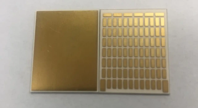
DBC (Direct Bonded Copper) substrates are designed for medium- and high-power modules and solve the challenge of directly bonding thick copper to ceramic.
- Bonding principle – At ~1065 °C in a controlled N₂/O₂ atmosphere, a Cu–O eutectic forms between the copper and Al2O3, creating a direct chemical bond.
- Key characteristics – Copper thickness from 100 µm up to 600 µm is feasible, providing very low interface thermal resistance and high current capability.
When qualifying a ceramic PCB manufacturer, verify their ability to inspect the DBC bonding interface (for example with Scanning Acoustic Microscopy, SAM) to ensure void-free thermal paths.
3. How to Evaluate and Select a Ceramic PCB Manufacturer
The choice of Al2O3 ceramic PCB manufacturer has a direct impact on reliability, lead time, and overall cost. Buyers should evaluate suppliers across several dimensions.
3.1 Deep-Dive into Technical Capabilities
| Evaluation Item | Key Requirements & Metrics | How to Verify in Practice |
|---|---|---|
| DBC/AMB bonding | Ability to provide non-destructive interface inspection (e.g., SAM) and low-void bonding. | Ask for DBC/AMB line photos and representative SAM inspection reports. |
| Thick-film capability | Line/space < 150 µm and laser-trimmed resistors with ±0.1 % accuracy. | Review equipment list and measured samples from laser-trimmed resistors. |
| Thin-film capability | Cleanroom class (e.g., Class 1000 or better) and fine lithography resolution. | Check cleanroom certification and the minimum feature size on samples. |
| Material control | Stable, traceable Al2O3 purity (96 % or 99.6 %). | Request material certificates and chemical composition reports. |
3.2 Quality Control and Reliability Assurance
Ceramic PCBs are often used in safety-critical systems, so a disciplined quality system is non-negotiable:
- Thermal cycling tests – For example, −40 °C to +150 °C for 1000 cycles to validate adhesion of DBC or thick-film metallization under thermal stress.
- Peel / pull strength testing – Routine testing to confirm metal-to-ceramic bond strength (often ≥ 20 N/mm²).
- Certifications – ISO 9001 is a baseline; for automotive applications, IATF 16949 is strongly preferred.
A true ceramic PCB manufacturer integrates these tests into the standard process flow rather than offering them as optional extras.
3.3 Cost Structure and Sourcing Strategy
The cost of an Al2O3 PCB is driven mainly by:
- Substrate material – Higher Al2O3 purity means higher cost and better performance.
- Metallization technology – Thin-film > DBC > thick-film in both performance and cost.
- Design complexity – Very small via diameters, high layer density, and complex outlines increase laser processing costs.
- Lot size – Ceramic PCBs have relatively high fixed tooling costs (masks, fixtures, etc.), so small-batch assembly has much higher unit cost than large-volume assembly.
A good sourcing strategy balances performance requirements with realistic volume forecasts and total cost of ownership.
4. Typical Application Segments for Al2O3 Ceramic PCBs
4.1 Automotive Electronics and EV Systems
In electric and hybrid vehicles, Al2O3 is widely used outside the very highest heat-flux points:
- On-board chargers (OBC) – Al2O3 DBC substrates provide the required power density and isolation to convert AC mains to DC for battery charging.
- Automotive lighting – High-power LED headlamps demand efficient heat spreading. Al2O3 ceramic PCBs are commonly used as LED bases to ensure long lifetime and color stability.
4.2 Aerospace and Defense
In satellite communications, radar front-ends, and avionics:
- High-frequency stability – The relatively low dielectric loss of Al2O3 supports signal integrity in L/S-band radar and communication links.
- Radiation tolerance – Ceramics maintain properties under ionizing radiation where many organic materials would degrade.
4.3 Hybrid Integrated Circuits (Hybrid ICs)
Al2O3 has been the foundation of hybrid IC technology for decades, enabling on a single substrate:
- Thick-film printed passive components – integrated resistor networks.
- Thin-film precision interconnects – microstrip lines and high-frequency transmission structures.
- Bare-die attach and wire bonding – for high-reliability sensor and control modules, including medical implants and industrial controllers.
5. Conclusion: Starting Your Al2O3 Ceramic PCB Project
Al2O3 ceramic PCBs are a robust building block for high-performance electronics. Their combination of thermal stability, electrical isolation, and thermo-mechanical compatibility makes them a compelling alternative to traditional rigid-flex PCBs and FR-4 in demanding environments.
Recommended next steps
- Clarify the required process – Based on power density and routing density, decide whether thick-film, thin-film, or DBC technology is the best fit.
- Define substrate specifications – Choose Al2O3 purity level (96 % vs. 99.6 %) and board thickness (for example 0.63 mm) according to mechanical and thermal needs.
- Engage with an experienced partner – Work with a ceramic PCB manufacturing specialist who offers end-to-end capabilities: design support, DFM review, metallization, precision laser processing, and reliability testing, all the way through to large-volume assembly.
With the right design choices and a capable manufacturing partner, Al2O3 ceramic PCBs can deliver the high reliability, thermal performance, and long-term stability that modern power and RF systems require.
Contact us today for a customized Al2O3 ceramic PCB solution and start your next high-reliability packaging project with confidence.
Common Questions
When is an Al2O3 ceramic PCB a better fit than FR-4 or a standard metal-core board?
It is often the better choice when the design needs a balanced mix of thermal conductivity, electrical insulation, temperature tolerance, and long-term reliability. That makes it especially relevant for power electronics, automotive modules, RF hardware, and high-voltage products.
How should a team choose between thick film, thin film, and DBC on Al2O3?
Thick film fits cost-sensitive designs that benefit from passive integration, thin film fits precision and RF structures, and DBC is usually the right direction for high-current power modules. The best answer depends on the electrical and thermal load, not on prestige.
If AlN has higher thermal conductivity, is it always better than Al2O3?
No. AlN offers a higher thermal ceiling, but it also brings higher cost and tighter supply and process demands. If the heat flux does not justify that jump, Al2O3 often provides the more practical performance-to-cost balance.
What should buyers verify first when sourcing Al2O3 PCBs?
They should verify substrate purity control, metallization competence, bond-interface inspection methods, and reliability test discipline such as thermal cycling. On ceramic boards, real process control matters far more than brochure claims alone.