
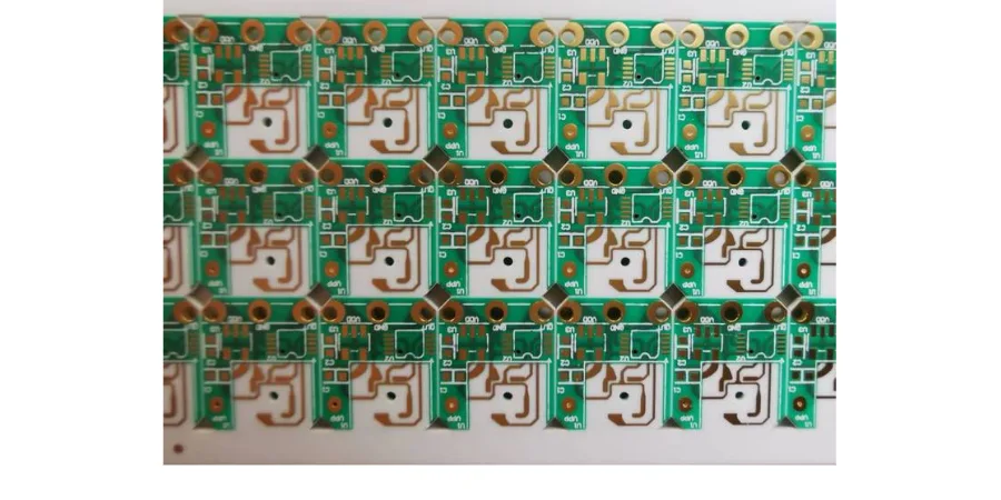
Highleap PCB Factory (HILPCB) manufactures alumina PCBs using aluminum oxide (Al2O3) ceramic substrates designed for applications that require high thermal conductivity, electrical insulation, mechanical stability, and long-term reliability.
Compared with conventional FR-4 PCB materials, alumina ceramic substrates provide superior heat dissipation and better dimensional stability at elevated temperatures. They are widely used in high-power LED modules, semiconductor packaging, automotive electronics, RF circuits, industrial controls, and power conversion systems.
HILPCB supports alumina PCB production from substrate processing and metallization to ceramic PCB assembly, including thick film, thin film, and direct bonded copper (DBC) technologies. Layout rules for these boards are covered in our Al2O3 PCB design guide.
Material Properties and Performance Characteristics of Alumina Substrates
Alumina (Al2O3) is the most widely adopted ceramic PCB substrate material because it provides a balanced combination of thermal performance, electrical insulation, mechanical strength, and manufacturing cost. Different alumina purity levels allow engineers to select the appropriate substrate performance for each application.
HILPCB provides multiple alumina grades based on thermal requirements, frequency performance, surface finish requirements, and reliability targets.
96% Alumina (Standard Grade)
- Thermal conductivity: 24-28 W/m·K
- Dielectric constant: 9.8 at 1 MHz
- Flexural strength: 380 MPa
- Volume resistivity: >10¹⁴ Ω·cm
- Cost-effective solution for general ceramic PCB applications
96% alumina is commonly selected for LED modules, power circuits, sensors, and industrial electronics where balanced thermal performance and cost control are required.
99.5% Alumina (High Purity Grade)
- Thermal conductivity: 30-35 W/m·K
- Surface finish: Ra <0.2μm
- Dielectric loss: tan δ <0.0002
- Improved mechanical strength and electrical performance
- Suitable for RF, microwave, and precision electronic applications
The higher purity reduces dielectric loss and improves surface quality, making 99.5% alumina suitable for circuits requiring stable electrical characteristics and fine conductor features.
99.9% Alumina (Ultra-Pure Grade)
- Thermal conductivity: 35-38 W/m·K
- Exceptional electrical insulation properties
- Porosity: <0.1%
- Used for advanced applications requiring maximum material performance
Ultra-pure alumina is selected for demanding semiconductor packaging, high-frequency circuits, and specialized industrial systems where material consistency is critical.
Alumina ceramic substrates have a thermal expansion coefficient of 6.5-7.5 ppm/K, which provides compatibility with semiconductor materials and reduces thermal stress during temperature cycling. The material also has zero moisture absorption, maintaining stable electrical and mechanical properties in humid environments.
For applications requiring high heat dissipation and electrical isolation, alumina substrates provide advantages over traditional FR-4 PCB designs.
Advanced Metallization Processes for Alumina Circuit Boards
Manufacturing reliable conductive patterns on ceramic substrates requires specialized metallization processes. HILPCB uses different metallization technologies based on circuit density, current requirements, frequency performance, and assembly method.
Thick Film Technology
Thick film processing uses screen printing to deposit conductive pastes onto alumina substrates. After printing, the substrate is fired at high temperature to create a durable conductor layer.
Key capabilities include:
- Conductor materials: Ag, AgPd, Au, Cu
- Standard line width/spacing: 100μm/100μm
- Minimum achievable line width/spacing: 75μm
- Multi-layer ceramic circuit capability with buried vias
- Integrated resistors and capacitors
- Firing temperature: 850-950°C
Thick film alumina PCBs are widely used in power electronics, LED applications, sensors, and industrial modules requiring reliable electrical performance.
Thin Film Processing
Thin film metallization provides finer circuit patterns and improved electrical performance for precision applications.
Process capabilities include:
- Sputtered Ti/Cu/Ni/Au metallization
- Feature sizes down to 25μm lines/spaces
- Titanium barrier layers for improved metal adhesion
- Compatibility with wire bonding and flip-chip assembly
- Controlled impedance capability for high-frequency PCB designs
Thin film alumina substrates are commonly used in RF modules, microwave circuits, semiconductor packages, and high-density electronic assemblies.
Direct Bonded Copper (DBC)
DBC technology bonds copper directly to ceramic substrates, creating a high-current circuit platform for power electronics.
Key advantages include:
- Copper thickness: 0.127mm to 0.4mm
- Current capacity exceeding 100A
- Excellent thermal cycling reliability
- Suitable for power module substrates
DBC alumina solutions support high-power semiconductor devices, including IGBT, SiC, and GaN components.

Manufacturing Excellence and Quality Control
HILPCB applies controlled ceramic PCB manufacturing processes to maintain consistency in substrate dimensions, metallization quality, and electrical performance.
Processing Capabilities
Our alumina PCB manufacturing capabilities include:
- Thickness range: 0.25mm to 3.0mm
- Camber tolerance: <0.05% of diagonal
- Surface finish options: As-fired, lapped, polished
- Laser drilling: 50μm minimum via diameter
Ceramic substrate processing requires precise handling because alumina provides excellent mechanical strength but remains more brittle than organic PCB materials. Manufacturing controls help prevent cracking, chipping, and dimensional variation.
Quality Assurance Measures
Every alumina circuit board undergoes inspection and testing procedures, including:
- Automated optical inspection for conductor pattern verification
- Cross-sectional analysis for layer thickness validation
- Adhesion testing exceeding MIL-STD-883 requirements
- Thermal resistance measurement for power applications
- 100% electrical testing for continuity and isolation
HILPCB operates an ISO 9001:2015 certified quality management system with production traceability from ceramic raw materials to finished alumina PCB products.
Applications and Assembly Services for Alumina PCBs
Alumina ceramic PCBs are selected for applications where standard PCB materials cannot provide sufficient thermal performance, electrical isolation, or environmental reliability.
Versatile Applications Across High-Reliability Fields
Medical Devices
Alumina substrates support medical electronics that require stable electrical insulation, chemical resistance, and long operational life. Applications include medical imaging equipment, patient monitoring systems, surgical electronics, and high-voltage medical assemblies.
The ceramic material is compatible with specialized metallization methods and supports applications requiring reliable performance under sterilization and environmental stress conditions.
LED and Lighting Systems
High-power LED designs generate significant heat that can reduce component lifetime if not managed effectively. Alumina PCBs provide a direct thermal path from LED components to the substrate.
Applications include:
- COB LED modules exceeding 150 lm/W
- UV-C sterilization LED arrays
- Automotive LED headlights
- Horticultural lighting systems
- High-power stadium lighting designed for extended service life
The combination of thermal conductivity and electrical insulation helps maintain LED efficiency and reliability.
Power Electronics and Energy
Alumina ceramic substrates are widely used in power electronics because they combine heat dissipation with electrical isolation.
Typical applications include:
- SiC and GaN power device packages
- Electric vehicle inverter modules
- Renewable energy converters
- Industrial motor drives
- High-voltage switching systems
Alumina boards support voltage ranges from 600V to over 1,000V and can operate reliably in long-life energy systems designed for 25+ years of service.
RF, Telecom, and Radar
Alumina provides stable dielectric characteristics required for high-frequency circuit performance.
Applications include:
- 5G power amplifier modules
- Satellite communication equipment
- Automotive radar systems operating at 77GHz
- Microwave circuits
- Hermetically sealed communication modules
- Compact IoT RF sensor devices
Low dielectric loss and consistent material properties make high-purity alumina suitable for RF and microwave applications.
Industrial and Harsh Environments
Alumina ceramic substrates maintain performance under high temperature, vibration, and chemical exposure.
Common applications include:
- High-temperature sensors operating up to 500°C
- Oil exploration electronics
- Aerospace avionics systems
- Factory automation equipment
- Industrial monitoring systems
The material’s thermal stability and mechanical strength support operation in demanding environments.
Specialized Assembly Services for Ceramic Substrates
HILPCB provides complete alumina PCB assembly services optimized for ceramic materials.
Available assembly processes include:
- Surface Mount Assembly (SMT) using ceramic-compatible thermal profiles and nitrogen reflow processes.
- Die attachment using gold-tin solder, sintered silver, or conductive epoxy based on thermal and electrical requirements.
- Wire bonding with gold or aluminum wires from 25-500μm diameter for fine-pitch and high-current applications.
- Flip-chip mounting with underfill materials selected for CTE matching and thermal stress reduction.
- Hermetic sealing for medical, aerospace, and military-grade electronic systems.
Additional reliability services include conformal coating, glob-top encapsulation, custom heat sink integration, EMI shielding, electrical testing, X-ray void inspection, and AOI verification.
Why Choose HILPCB for Alumina PCB Manufacturing
Choosing the right alumina PCB manufacturer requires experience with ceramic material processing, metallization methods, and assembly requirements. HILPCB supports customers from prototype development through volume production with engineering assistance focused on manufacturability and reliability.
Our ceramic PCB services include:
- Alumina substrate selection based on thermal and electrical requirements
- DFM optimization before production
- Prototype production in 7-10 days for selected designs
- Large-volume assembly with monthly capacity exceeding 100,000 units
- Ceramic-safe packaging for global shipment
- Technical support during assembly process development
Our engineering team helps optimize trace design, metallization selection, thermal management structures, and assembly methods to reduce production risks.
For applications requiring high thermal performance, stable dielectric properties, or long-term reliability, HILPCB provides alumina PCB solutions for LED systems, power modules, RF electronics, and industrial equipment.
Frequently Asked Questions
What advantages do alumina PCBs offer over metal core PCBs?
Alumina PCBs provide electrical insulation directly through the ceramic substrate without requiring additional dielectric layers used in many metal core PCB structures. Alumina offers 24-35 W/m·K thermal conductivity while maintaining volume resistivity above 10¹⁴ Ω·cm. Its thermal expansion coefficient also better matches semiconductor materials, reducing mechanical stress during thermal cycling.
How do 96% and 99% alumina compare for different applications?
96% alumina provides a cost-effective solution for general LED, sensor, and power applications with thermal conductivity of 24-28 W/m·K. Higher purity alumina grades, such as 99.5%, provide improved thermal conductivity of 30-35 W/m·K, lower dielectric loss, and better surface finish for RF and precision electronic applications.
What are typical lead times for alumina PCB orders?
Standard alumina PCB prototypes typically ship within 10-12 days. Selected quick-turn designs can be completed in 7 days. Complex assemblies involving wire bonding, special metallization, or additional testing usually require 15-20 days. Alumina substrate inventory helps reduce material sourcing delays.
Can alumina substrates be laser drilled for vias?
Yes. HILPCB uses CO2 and UV laser drilling processes to create ceramic vias with minimum diameters of 50μm. Laser drilling reduces mechanical stress compared with conventional drilling methods and enables clean, reliable via structures. Available options include filled vias for thermal management and castellated vias for edge connections.
What design guidelines apply to alumina PCB layouts?
Typical alumina PCB design guidelines include:
- Minimum trace width: 100μm for thick film and 25μm for thin film processes
- Minimum via diameter: 100μm
- Edge clearance: 0.5mm to reduce chipping risk
- Corner radius: >0.2mm
HILPCB provides DFM reviews to verify ceramic PCB designs before production.
How do you handle the brittleness of alumina during assembly?
Alumina PCB assembly requires specialized handling methods to prevent mechanical damage. HILPCB uses substrate support fixtures, controlled heating and cooling profiles, reduced vacuum pressure, and ceramic-compatible placement tooling. These processes protect ceramic substrates while maintaining reliable assembly yields.