
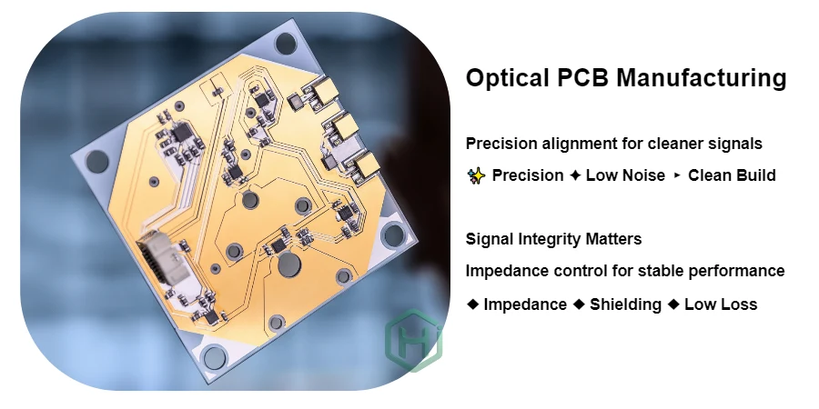
With AI and cloud computing accelerating, data-center traffic is growing exponentially, pushing optical modules toward 800G, 1.6T, and beyond. In this wave, the automotive-grade TIA/LA receiver board is a core building block whose design and manufacturing complexity—and importance—keep rising. It is not only the key platform that carries opto-electrical conversion, but also the main battleground for stringent thermal management, high-speed signal integrity, and long-term reliability. As an engineer focused on MT Ferrule and fiber routing, I know that even a small PCB-level defect can cause a sharp increase in coupling loss or signal distortion, ultimately degrading end-to-end link performance. This article dives into the core challenges of building a high-performance automotive-grade TIA/LA receiver board, and shares practical design strategies and manufacturing considerations.
A well-designed TIA/LA receiver board must achieve balance across optical, electrical, thermal, and mechanical dimensions. From sub-micron alignment between the fiber array and detectors, to high-speed signaling around the TIA/LA, to power and cooling under dense QSFP-DD/OSFP packaging, every step places demanding requirements on PCB design and fabrication. This is not only a technical issue—it directly impacts TIA/LA receiver board cost optimization and the feasibility of volume production.
Opto-electrical co-design: precision alignment and coupling between TIA/LA and fiber arrays
On the receive side of an optical module, the first job is to couple light carried by fibers efficiently and accurately onto the photodiode (PD) array, then convert and amplify it with a transimpedance amplifier (TIA) and a limiting amplifier (LA). Success depends directly on sub-micron alignment among the fiber array, lens array, and PD array.
PCB mechanical stability is the foundation
In this system, the automotive-grade TIA/LA receiver board PCB acts as the “optical platform.” Any PCB warpage or deformation caused by temperature change, mechanical stress, or material aging can break the designed optical alignment, reducing coupling efficiency and increasing channel-to-channel crosstalk. Therefore, the first step of TIA/LA receiver board best practices is choosing a substrate with excellent dimensional stability. For example, low Z-axis CTE (coefficient of thermal expansion) materials can significantly reduce Z expansion, improving long-term BGA joint reliability. A strictly symmetric stackup is also essential for warpage control—it balances internal stress generated during thermal cycling.
Signal integrity and fiber routing
From my domain perspective, internal fiber routing is just as important as high-speed electrical routing on the PCB. An improper bend radius increases macrobend loss, and fiber crossings can introduce stress. PCB design must reserve sufficient and sensible space for fiber components, avoiding interference with high-speed differential pairs or power planes. In the TIA/LA receiver board prototype phase, co-design via 3D modeling should validate optical and electrical placement so they don’t conflict. In addition, the transmission path from TIA/LA output to the connector is highly sensitive to PCB dielectric constant (Dk) and loss factor (Df). Choosing High Speed PCB materials such as Megtron 6 or Tachyon 100G is foundational for PAM4 eye quality and jitter suppression.
TEC and thermal-path co-design: system-level thermal management from chip to heatsink
As per-lane data rates rise to 100Gbps and even 200Gbps, TIA/LA power density increases sharply, often reaching several watts. For DWDM systems that require precise wavelength control, laser and detector temperature must be held within a tight window, typically with a thermoelectric cooler (TEC). An efficient thermal system is the lifeline for long-term stable operation of an automotive-grade TIA/LA receiver board.
Build a seamless vertical thermal path
The best thermal design creates a low-thermal-resistance “highway” from the chip to the external heatsink. A typical path is: TIA/LA chip -> thermal interface material (TIM) -> PCB copper / copper coin -> thermal via array -> PCB bottom -> module housing / heat spreader.
- Thermal via array: the key for moving heat through the PCB core dielectric. Optimize via diameter, pitch, copper plating thickness, and whether to fill with thermal material. A dense array behaves like a high-thermal-conductivity metal column, dramatically reducing vertical thermal resistance. When building High Thermal PCB, uniform and complete via plating is critical.
- Copper coin / embedded copper block: for very high-power chips, embed a solid copper coin inside the PCB to contact the die underside directly, providing a far more efficient thermal path than vias. This is one of the TIA/LA receiver board best practices, but it demands advanced manufacturing control.
TEC control and thermal isolation
With TEC, the PCB must separate the “hot side” and “cold side” effectively. A “thermal isolation zone” is usually created around the TEC—often by slots or low-thermal-conductivity structures—to prevent heat from flowing back to the cold side and reducing TEC efficiency. Power traces for the TEC must be wide enough for higher current, and their Joule heating must be included in the overall thermal model. A successful TIA/LA receiver board prototype must validate thermal design through detailed simulation and IR thermography.
HILPCB manufacturing capabilities: precision thermal-management PCBs
| Technical parameter | HILPCB capability | Value for TIA/LA Receiver Boards |
|---|---|---|
| Thermal via filling | Conductive/non-conductive resin fill, planarity < 1 mil | Maximizes heat transfer efficiency and provides a reliable soldering surface for BGA. |
| Embedded copper coin | Multiple sizes/shapes supported, high lamination registration | Best-in-class localized cooling solution for high-power TIA/LA chips. |
| High-thermal-conductivity materials | 2–10 W/mK substrate options available | Reduces overall thermal resistance at the material level and improves heat distribution. |
| Stackup symmetry control | Warpage controlled within 0.5% | Maintains optical alignment accuracy and improves assembly yield. |
CTE matching and low warpage: core strategies for material selection and stackup design
CTE mismatch is one of the primary root causes of failures in high-density electronic packaging. On an automotive-grade TIA/LA receiver board, the TIA/LA die (often silicon or III-V, CTE ~3–6 ppm/°C) and the PCB substrate (traditional FR-4 CTE ~14–18 ppm/°C) have a large CTE gap. During reflow and operational temperature cycling, the mismatch becomes mechanical stress concentrated at BGA or flip-chip joints, eventually causing solder fatigue cracking.
Using low-CTE materials
To mitigate this, selecting low-CTE PCB materials is key. Some hydrocarbon or PTFE-based substrates designed for high-speed applications can keep in-plane CTE below 10 ppm/°C, closer to semiconductor dies. For extreme reliability, Ceramic PCB (e.g., alumina or aluminum nitride) is ideal: CTE matches die materials well and thermal performance is excellent. However, it increases cost significantly and must be weighed carefully in TIA/LA receiver board cost optimization.
The art of stackup design
Beyond the material itself, stack structure is critical for warpage control. A core principle is “symmetry”:
- Structural symmetry: dielectric thickness, copper thickness, core type, etc. should be mirror-symmetric about the PCB center.
- Copper distribution symmetry: copper coverage across signal and power layers should be as even and symmetric as possible, avoiding large local density differences that create uneven lamination stress.
Well-designed stackups minimize warpage while improving impedance control and crosstalk performance—prerequisites for reliable TIA/LA receiver board mass production.
PAM4 high-speed link power and power integrity challenges
The shift from NRZ to PAM4 doubles data rate at the same baud rate, but introduces tougher SI and PI constraints. PAM4 has a smaller vertical eye height and narrower horizontal eye width, making it far less tolerant to noise, jitter, and nonlinear distortion.
A robust power distribution network (PDN)
TIA/LA devices are mixed-signal (analog + digital) and extremely sensitive to supply noise. Any rail fluctuation can directly modulate the amplified high-speed signal, causing eye closure and higher bit error rate (BER). A low-impedance, low-noise PDN is therefore essential.
- Plane capacitance: tightly coupled power and ground planes provide natural plane capacitance and a low-impedance return path for high-frequency current.
- Decoupling capacitors: carefully place multi-value decap arrays near the power pins. Small-value, small-package capacitors (0201/01005) serve high-frequency decoupling, while larger values provide mid/low-frequency charge storage. Placement and via breakout strongly affect decoupling effectiveness.
- Power isolation: physically isolate sensitive analog supplies (e.g., TIA front-end) from noisy digital supplies (e.g., LA logic or DSP) using split planes or ferrites/filters.
A strong PDN is the foundation for stable operation in harsh EMI environments, and a key step from prototype validation to volume production.
PAM4 power integrity design essentials
- Target impedance: across the target frequency range (typically from a few kHz to several GHz), PDN impedance must stay below the defined target to suppress voltage ripple.
- Cap selection and placement: use multi-stage decoupling. ESL matters more than capacitance value—place caps as close as possible to the power pins.
- Return path control: ensure every high-speed signal has a continuous, low-inductance ground return; avoid return-current switching between planes.
- Co-simulation: perform SI/PI co-simulation to quantify the impact of supply noise on eye diagrams and optimize early.
Airflow and cooling options: thermal considerations for QSFP-DD/OSFP modules
Optical modules are ultimately integrated into QSFP-DD or OSFP pluggable form factors and densely packed on switch front panels. Their thermal performance depends heavily on forced airflow provided by the system. Automotive-grade TIA/LA receiver board design must consider module-level airflow organization.
Internal air channeling and pressure drop (ΔP)
The heatsink fins on the module shell are the main interface for heat exchange with external airflow. But internal heat transfer to the shell is equally critical. Component placement on the PCB shapes small internal airflow channels. Tall components can block airflow and create downstream hot spots. Place high-power devices (TIA/LA, DSP) upstream in the airflow path or keep sufficient clearance around them. The module airflow resistance—pressure drop (ΔP)—is a key system parameter. Excessive ΔP reduces actual airflow through the module and degrades cooling.
Selecting advanced cooling technologies
For next-generation optical modules above 20W, traditional air cooling may reach its limit. More advanced approaches may be required:
- Heat pipes / vapor chambers (VC): passive two-phase devices with extremely high effective thermal conductivity, spreading heat rapidly from the chip region across the heatsink surface and eliminating hot spots.
- Liquid cooling: integrating microchannels and using liquid coolant can remove orders of magnitude more heat than air. This is considered the ultimate solution for future ultra-high-power optical modules, but introduces new challenges in sealing, coolant compatibility, and cost control.
For TIA/LA receiver board cost optimization, select the best cooling approach based on module power budget, environment, and target cost.
From prototype to volume production: testing, validation, and design for manufacturing (DFM)
A successful automotive-grade TIA/LA receiver board must pass rigorous validation and incorporate DFM from day one to ensure a smooth transition from TIA/LA receiver board prototype to TIA/LA receiver board mass production.
A comprehensive test and validation system
- Thermal tests: use IR thermography to measure temperature distribution under different power levels and ambient conditions. Test module thermal performance in a wind tunnel at different airflow speeds to extract actual thermal resistance.
- Signal integrity tests: use VNA to measure S-parameters (insertion loss, return loss), and use a high-bandwidth oscilloscope plus BERT to test PAM4 eye, TDECQ, jitter, and other key metrics.
- Reliability tests: run thermal cycling, temperature-humidity-bias, vibration/shock, and other environmental stress tests to simulate lifecycle extremes and validate long-term reliability.
DFM and supply-chain collaboration
DFM bridges design and manufacturing. Working closely with PCB fabs and assemblers (such as HILPCB) during design avoids many late-stage issues—materials availability, stackup manufacturability, BGA pad rules, test-point placement, and more. A strong partner provides not only quality manufacturing, but also early optimization guidance—critical for TIA/LA receiver board cost optimization and time-to-market. HILPCB’s prototype assembly service enables fast early iteration and validation, forming a solid foundation for TIA/LA receiver board mass production.
Conclusion
Designing and manufacturing a high-performance, high-reliability automotive-grade TIA/LA receiver board is complex systems engineering that spans optics, electronics, thermals, and mechanics. From mechanical stability that protects optical alignment, to detailed thermal-path design that manages chip power; from symmetric stackup strategies that suppress warpage, to robust PDN design that protects PAM4 signal quality—every detail determines optical-module performance and reliability.
As data centers move toward higher speeds and higher density, requirements for TIA/LA receiver boards will only become more demanding. Only by adopting advanced materials, deliberate co-design, rigorous test validation, and deep collaboration with experienced manufacturing partners can we meet these challenges and build the solid physical foundation that keeps the future digital world running at full speed.