
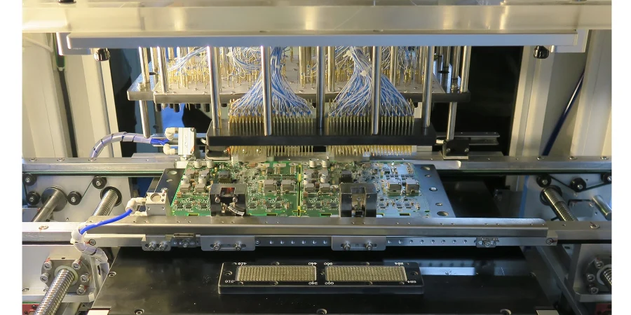
For AI accelerators, chiplets, HBM systems, and dense IC substrate PCB designs, the key decision is not whether to use Boundary-Scan/JTAG—it is where it fits in the complete validation strategy. Engineers should decide whether JTAG will be used only for production test, or as a lifecycle diagnostic path covering design validation, manufacturing, bring-up, and field service. The evidence required before supplier selection includes scan-chain architecture, BSDL availability, DFT review results, high-speed PCB material data, cross-section reports, and verification of assembly processes.
As package density increases, physical probing becomes less practical. Dense BGA arrays, buried vias, and advanced packaging structures make traditional test access difficult. Boundary-Scan/JTAG provides digital access to interconnects through IEEE 1149.1 architecture, helping teams verify connections that cannot be reached by conventional probes.
For AI hardware procurement, the manufacturing partner decision should be based on measurable test capability—not only fabrication capability.
What does Boundary-Scan/JTAG verify in AI chip interconnect designs?
Boundary-Scan/JTAG inserts boundary cells between IC pins and internal logic. These cells connect into a scan chain controlled through the Test Access Port (TAP).
The TAP interface includes:
- TCK (Test Clock): synchronizes scan operations.
- TMS (Test Mode Select): controls TAP state transitions.
- TDI (Test Data In): transfers serial test data into the chain.
- TDO (Test Data Out): transfers serial test data out.
- TRST (Test Reset): optional asynchronous TAP reset.
Important JTAG instructions include:
- EXTEST: verifies external PCB connections, including solder joints, traces, vias, and device-to-device links.
- SAMPLE/PRELOAD: captures or loads boundary states.
- IDCODE: confirms device identity and assembly correctness.
- BYPASS: removes devices from active scan operations.
- INTEST: supports internal logic testing.
For high-density AI boards, JTAG acts as a virtual probe. It does not replace signal integrity or power integrity analysis, but it confirms that the physical connection foundation is correct before engineers spend time analyzing SI/PI failures.
When should AI hardware teams choose JTAG over ICT or flying probe testing?
Traditional ICT and flying probe testing depend on physical access. Modern AI hardware frequently limits that access through:
- Large BGA packages.
- Fine-pitch package escape routing.
- HDI structures.
- Buried interconnects.
- Multi-die packaging.
A design using HDI PCB technology may require Boundary-Scan/JTAG because adding physical test points can consume routing space needed for impedance control and power distribution.
| Test method | Physical access requirement | BGA/high-density suitability | Best evidence for supplier evaluation |
|---|---|---|---|
| Boundary-Scan/JTAG | TAP access only | High for hidden connections | BSDL coverage report, scan-chain validation, fault diagnostics |
| ICT | Multiple test points and fixture access | Reduced for dense packages | Fixture design, test coverage report |
| Flying probe | Probeable pads, vias, or exposed nets | Limited by access density | Probe strategy, net coverage analysis |
The correct decision is usually not JTAG versus ICT. High-reliability products often combine methods: JTAG for structural connectivity, X-ray for hidden solder inspection, and functional testing for system behavior.
How should engineers estimate JTAG test coverage by BGA pitch?
JTAG coverage depends heavily on the physical access available around fine-pitch BGA packages. As pitch decreases, probeable pads and test points become scarcer, making boundary-scan a larger share of the overall test strategy. The following estimator table maps BGA pitch to expected JTAG coverage, physical access level, complementary test methods, and BSDL file requirements.
| BGA pitch | Physical access | JTAG coverage estimate | Recommended complementary test | BSDL requirement |
|---|---|---|---|---|
| 0.4 mm | Very limited | 70–85% | X-ray + ICT | Required |
| 0.5 mm | Limited | 75–90% | X-ray + flying probe | Required |
| 0.65 mm | Moderate | 80–95% | Flying probe + FCT | Recommended |
| 0.8 mm | Good | 85–95% | ICT + FCT | Optional |
| 1.0 mm | Full | 90–98% | FCT | Optional |
Engineers should treat the coverage estimates as planning ranges, not guarantees. Actual coverage depends on scan-chain completeness, the percentage of nets connected to JTAG-capable devices, and whether BSDL files are available for every boundary-scan device on the board. At finer pitches where physical access is very limited, JTAG becomes the primary structural test method and complementary X-ray inspection fills the gap for hidden solder joint verification.
What technical parameters affect Boundary-Scan/JTAG reliability?
JTAG itself operates at lower frequencies than high-speed data links, but the surrounding PCB environment determines whether the test strategy succeeds. AI hardware must simultaneously manage connectivity, power delivery, thermal behavior, and signal integrity.
| Parameter | Typical engineering value | Decision impact | Evidence to request |
|---|---|---|---|
| JTAG clock frequency | 10–50 MHz typical design range | Poor routing can create test failures | JTAG routing review |
| High-speed links | PCIe 6.0, HBM3e, CXL-class interfaces | Physical defects can appear as SI failures | SI simulation and validation data |
| Thermal conductivity | 1.5–3 W/mK standard dielectric; 4–8 W/mK high-performance thermal materials | Determines heat spreading capability | Material datasheet and thermal test report |
| Copper weight | Common PCB values include 1 oz and higher for power layers | Affects current capacity and PDN design | Stackup and copper specification |
| Dielectric constant (Dk) | Controlled by laminate selection; high-speed materials commonly provide specified Dk values at operating frequency | Controls impedance and propagation delay | Material datasheet with Dk test conditions |
| Via diameter | HDI microvias commonly use tens to hundreds of µm; designs may specify values such as 100 µm class structures | Determines escape routing density | Via drawing and cross-section |
| Temperature capability | Material systems commonly evaluated for operating ranges around 125°C or higher depending on application | Impacts reliability in AI and industrial systems | Thermal cycling data |
A supplier that cannot provide stackup details, material data, and manufacturing evidence creates unnecessary risk for high-value AI hardware.
How does JTAG support high-speed SI and PI debugging?
Boundary-Scan/JTAG does not measure eye diagrams, jitter, insertion loss, or voltage ripple. Instead, it answers an earlier question:
Is the physical connection correct?
For example, a failed HBM channel may be caused by:
- BGA solder defects.
- Open vias.
- Trace discontinuities.
- Power delivery problems.
- Signal tuning issues.
JTAG can eliminate open and short defects before engineers investigate advanced SI/PI causes. This reduces debugging scope because teams know whether the failure is physical connectivity or system performance.
For high-speed PCB projects, the JTAG decision should be integrated with fabrication requirements such as controlled impedance, HDI capability, and stackup control. A High-Speed PCB supplier should demonstrate how manufacturing controls support the electrical validation process.
What should engineers review during DFM/DFT/DFA before production?
A successful Boundary-Scan/JTAG implementation begins before PCB fabrication.
The DFM/DFT/DFA review should verify:
Scan-chain topology
- Device order.
- TDI-to-TDO continuity.
- Multi-device chain strategy.
- FPGA, CPLD, and processor programming access.
BSDL availability
- Every JTAG-capable device should have the correct Boundary Scan Description Language file.
- Missing BSDL files can prevent automated test development.
JTAG routing
- TCK, TMS, TDI, and TDO require controlled routing practices.
- Long or noisy routes can create false failures even at 10–50 MHz.
Production access
- TAP connectors or test access points must remain available after assembly, enclosure integration, or potting/encapsulation.
How does potting or encapsulation change the JTAG decision?
Potting improves environmental protection against moisture, vibration, chemicals, and temperature stress. However, it also removes physical repair access.
For encapsulated products, JTAG should be treated as a lifecycle interface.
It enables:
- Field diagnostics without destructive teardown.
- Firmware updates through supported programming workflows.
- Verification after deployment.
- Separation of interconnect failures from software failures.
The TAP interface must be planned before encapsulation. Once epoxy or silicone materials cover the assembly, adding access later may be impossible.
Which manufacturing evidence should procurement request before selecting a supplier?
Procurement teams should request technical evidence that proves the supplier can manufacture and test the design.
Required RFQ submission package:
Customer design files to submit
- Gerber files or ODB++ manufacturing package.
- Complete BOM.
- PCB stackup specification.
- Controlled impedance requirements.
- Via drawing.
- Drill files.
- Pick-and-place files.
- Assembly drawings.
- JTAG chain documentation.
- BSDL files for supported devices.
- Test requirements.
- Functional test specifications.
Supplier evidence to request
- DFM/DFT/DFA review report.
- PCB cross-section analysis.
- Material datasheets.
- Copper thickness verification.
- Thermal test report when thermal management is critical.
- X-ray inspection capability for hidden BGA joints.
- JTAG test coverage report.
- Failure analysis documentation.
- SMT process documentation.
A complete turnkey PCBA solution should connect fabrication, assembly, programming, inspection, and electrical test into one controlled workflow.
What are the main failure modes JTAG helps diagnose?
| Failure mode | Likely root cause | Verification method |
|---|---|---|
| Open BGA connection | Solder void, head-in-pillow defect, insufficient solder connection | JTAG EXTEST, X-ray inspection, cross-section |
| Short between nets | PCB fabrication defect, solder bridge, assembly contamination | Boundary scan shorts test, AOI, electrical isolation test |
| Incorrect device population | Wrong component, placement error, missing device | IDCODE scan, BOM verification |
| Broken scan chain | Incorrect routing, damaged trace, failed device | TAP continuity test, chain analysis |
| High-speed channel instability | SI issue, impedance discontinuity, power noise | JTAG connectivity check followed by SI/PI analysis |
| Field failure after encapsulation | Hidden interconnect or firmware issue | External JTAG diagnostics |
How should engineers select a PCB partner for AI interconnect projects?
The right supplier is not simply the one with the highest layer count or lowest quote. AI hardware requires coordination between PCB fabrication, IC substrate PCB capability, assembly precision, and test engineering.
A qualified partner should demonstrate:
- Early DFT involvement during design review.
- Experience with dense BGA and HDI structures.
- JTAG integration into SMT assembly workflows.
- Ability to provide manufacturing evidence.
- Complete traceability from components through final test.
For IC substrate PCB projects, the supplier must understand that electrical performance depends on the complete path from package escape routing to board-level interconnect.
Conclusion: What should teams decide before starting an AI PCB project?
Boundary-Scan/JTAG should be treated as a design decision, not a production afterthought. It provides essential visibility when physical access disappears and helps engineers separate manufacturing defects from complex SI/PI challenges.
Before approving a supplier, confirm:
- The scan chain architecture is defined.
- BSDL files are available.
- DFT review is complete.
- High-speed material and stackup data are documented.
- Production evidence can be provided.
For advanced AI hardware, JTAG is the connection between design confidence, manufacturing verification, and long-term product reliability.
Common Questions
Why is Boundary-Scan/JTAG important for AI chip interconnect?
AI hardware uses dense packages and limited physical access. Boundary-Scan/JTAG provides digital access to verify connections that conventional probes may not reach.
Can JTAG replace signal integrity testing?
No. JTAG verifies connectivity and structural integrity. SI analysis is still required for high-speed links such as HBM3e, PCIe 6.0, and CXL-class designs.
What files are required for JTAG production testing?
Typical requirements include PCB manufacturing files, BOM, stackup, assembly drawings, JTAG chain information, and BSDL files.
Why does JTAG matter after potting or encapsulation?
Because physical repair becomes difficult after encapsulation. A planned JTAG interface enables diagnostics and firmware maintenance throughout the product lifecycle.