
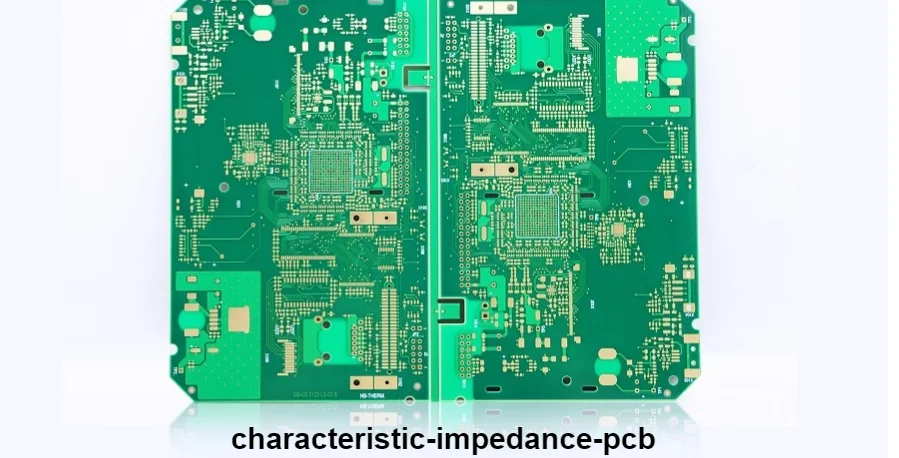
A controlled impedance PCB is a printed circuit board whose specified transmission-line structures are designed and manufactured to meet target characteristic impedance values within defined tolerances. The target is achieved through a coordinated stackup, trace geometry, material system, fabrication process, and verification plan—not by trace width alone.
This guide helps design and sourcing teams specify what the fabricator must control and test.
Key Takeaways
- Characteristic impedance is determined by the trace and its electromagnetic environment, including reference planes, geometry, dielectric properties, copper thickness, and nearby conductors.
- Fast edge rate—not clock frequency alone—determines when a digital interconnect behaves as a transmission line.
- A field-solver result is a design prediction; a TDR measurement on a representative coupon is manufacturing evidence. Neither replaces system-level signal-integrity validation.
- The fabrication drawing should identify impedance type, target, tolerance, layer, reference plane, trace width, and differential spacing.
- Let the fabricator review the stackup before layout is frozen.
What Is Characteristic Impedance in a PCB?
Characteristic impedance, commonly written as Z0, is the voltage-to-current relationship of a traveling wave on a transmission line. A PCB trace becomes a transmission line when its propagation delay is significant relative to the signal transition time. Discontinuities then cause part of the wave to reflect, which can reduce timing or voltage margin and increase ringing or EMI.
The relevant structure is not just copper. A microstrip uses an outer-layer trace and a reference plane; a stripline is routed between reference planes; a coplanar structure also depends on nearby same-layer copper. Differential impedance depends on both each trace-to-plane relationship and coupling between the pair.
Common interface specifications often call for values such as 50Ω single-ended or 90Ω, 100Ω, and other differential targets, but the interface standard and device guidance—not convention—must define the actual requirement.
When Does a PCB Need Controlled Impedance?
Controlled impedance is normally considered for fast digital interfaces, RF and microwave paths, clocks, memory buses, high-speed connectors, and other nets where reflections or loss can consume the available channel margin. A low clock rate does not automatically make a trace electrically slow: a device with a fast output edge can excite high-frequency behavior even when it switches infrequently.
Use edge rate, interconnect delay, topology, termination, channel budget, and EMC risk to decide which nets require control. Short local GPIO traces may not need a callout, while PCIe, USB, Ethernet, HDMI, DDR, and RF paths generally follow interface and component guidance.
Controlled impedance also does not mean “match every trace to 50Ω.” The source, load, termination network, connector, cable, and PCB channel must be considered as a system.
Which Variables Control PCB Trace Impedance?
The table below gives useful directional relationships, but it is not a substitute for a field solver. Real stackups may include trapezoidal etched traces, multiple dielectrics, solder mask, frequency-dependent material properties, and copper roughness.
| Variable | Typical effect when other variables stay fixed | Manufacturing concern |
|---|---|---|
| Trace width increases | Impedance decreases | Etch compensation and finished width vary by copper layer/process |
| Copper thickness increases | Impedance usually decreases | Base copper plus plating affects outer-layer geometry |
| Distance to reference plane increases | Impedance increases | Pressed dielectric thickness depends on laminate/prepreg construction |
| Dielectric constant increases | Impedance decreases | Use material data appropriate to the model and frequency |
| Differential-pair spacing decreases | Differential impedance generally decreases | Etch and registration affect the finished gap |
| Coplanar ground moves closer | Impedance generally decreases | Copper clearance and solder-mask assumptions must match fabrication |
| Solder mask is added | Outer-layer impedance usually decreases slightly | Mask thickness and dielectric behavior may need inclusion in the model |
At higher frequencies, dielectric loss, copper roughness, skin effect, and dispersion also affect channel behavior. “FR-4 up to a certain GHz” is not a reliable selection rule because trace length, loss budget, construction, temperature, and cost all matter.
How Should Designers and Fabricators Develop the Stackup?
- Identify controlled nets, interface standards, target impedance, tolerance, and maximum channel loss where relevant.
- Define layer count, signal/reference-plane relationships, copper needs, overall thickness, via strategy, and material constraints.
- Ask the fabricator for a buildable stackup based on available cores, prepregs, resin fill, copper, and process capability.
- Calculate trace width and spacing with a field solver using the agreed finished construction.
- Review breakout, reference transitions, via stubs, connector launches, plane voids, and return-via placement.
- Put the final impedance table and test requirement on controlled fabrication documentation.
- Resolve any proposed width, spacing, material, or stackup adjustment through documented engineering approval.
For multilayer PCB or HDI PCB, electrically possible geometry must still satisfy fabrication, current, loss, and reliability requirements.
What Should a Controlled Impedance Drawing Specify?
An impedance callout should remove ambiguity about both the structure and the acceptance test. A useful table looks like this:
| ID | Layer | Structure | Reference plane(s) | Target | Tolerance | Nominal finished width | Pair gap | Test |
|---|---|---|---|---|---|---|---|---|
| Z1 | L1 | Single-ended microstrip | L2 | 50Ω | As specified | Per approved stackup | N/A | TDR coupon |
| Z2 | L3 | Differential stripline | L2/L4 | 100Ω differential | As specified | Per approved stackup | Per approved stackup | TDR coupon |
Replace the examples with actual interface requirements. State whether dimensions are design or finished values, whether solder mask is included, document precedence, and whether the fabricator may adjust geometry after approval.
A blanket note such as “all high-speed traces 50Ω” is inadequate. It does not identify net classes, differential requirements, layers, references, tolerances, or verification.
How Is Controlled Impedance Verified With TDR Coupons?
Time-domain reflectometry sends a fast edge into a transmission line and observes reflections over time. PCB fabricators commonly measure purpose-built coupons located on the production panel because a coupon provides accessible, repeatable test structures designed to represent specified board layers and constructions.
The coupon represents a process and geometry; it does not prove every routed feature. The drawing or quality agreement should define coupon structures, panel sampling, tolerance, reporting, and lot disposition.
Three terms are often confused:
| Approach | What is controlled or delivered | Appropriate evidence |
|---|---|---|
| Calculated impedance | Geometry is designed to a modeled target | Approved stackup and field-solver result |
| Controlled dielectric | Material and dielectric construction are built to specified requirements | Stackup/material and thickness records |
| Controlled impedance | Defined structures must meet a target and tolerance | TDR coupon result plus agreed fabrication records |
VNA and S-parameter measurements answer frequency-domain loss and reflection questions but require suitable fixtures, calibration, structures, and a separate test plan. Neither TDR nor VNA guarantees system compliance.
Which Layout Errors Break Impedance Continuity?
| Risk | Why it matters | Typical review action |
|---|---|---|
| Split or void in reference plane | Interrupts the return-current path | Reroute over a continuous reference or redesign the transition |
| Layer-change via without nearby return path | Forces return current through a larger loop | Add suitable ground return vias based on the stackup and interface |
| Long via stub | Creates a frequency-dependent resonant discontinuity | Review layer assignment, via structure, or backdrilling when justified |
| Pair spacing changes or asymmetry | Changes coupling and conversion between differential/common modes | Keep pair geometry consistent except for analyzed breakout regions |
| Connector or BGA escape | Creates a local geometry change | Model or review the launch with package/connector data |
| Copper pour too close to a trace | Changes a nominal microstrip into a coplanar structure | Apply a modeled clearance, not an arbitrary rule |
| Unapproved stackup substitution | Changes dielectric height and material properties | Require engineering review before fabrication |
For high-speed PCB and high-frequency PCB, impedance is only one part of a channel budget that also includes loss, crosstalk, skew, vias, and connectors.
Controlled Impedance PCB RFQ Checklist
Provide the following with the quotation package:
- Gerber or ODB++ data, drill files, netlist, fabrication drawing, and revision history
- layer count, overall thickness, copper weights, surface finish, and material constraints
- impedance table listing target, tolerance, layer, structure, reference plane, nominal width, and pair gap
- governing interface or device requirements and any loss target
- approved stackup or permission for HILPCB to propose a stackup for review
- solder-mask assumptions and finished-dimension conventions
- coupon design/ownership, TDR sampling, report format, and lot acceptance rules
- special structures such as blind/buried vias, via-in-pad, backdrilling, rigid-flex transitions, or edge launches
- quantity, panel restrictions, inspection documentation, and change-approval requirements
How Can HILPCB Support Controlled Impedance PCBs?
HILPCB supports controlled-impedance fabrication through stackup and DFM review, geometry feedback, manufacturing controls, and scoped verification, including rigid-flex PCB builds where applicable.
Capability depends on layer construction, finished copper, geometry, target and tolerance, materials, panel design, and test method. Send the impedance table before layout release.
Reference Standards and Scope
- IPC-2141A — Design Guide for High-Speed Controlled Impedance Circuit Boards
- IPC-2221 — Generic Standard on Printed Board Design
- IPC-6012 — Qualification and Performance Specification for Rigid Printed Boards, where applicable
- IPC-TM-650 2.5.5.7A — Characteristic Impedance Lines on Printed Boards by TDR
The customer or product owner remains responsible for interface requirements, simulation assumptions, termination strategy, channel compliance, EMC, environmental qualification, and system-level validation. PCB coupon results demonstrate the agreed fabrication characteristic; they do not certify the complete electronic product.
Frequently Asked Questions
What is the difference between characteristic impedance and resistance?
DC resistance describes conductor loss under steady current. Characteristic impedance describes the voltage-to-current relationship of a traveling wave on a transmission line and depends on distributed inductance and capacitance. A PCB trace can have low DC resistance while still having a specified 50Ω characteristic impedance.
Is ±10% the standard impedance tolerance?
±10% is a common commercial request, but it is not universal. Tighter or different tolerances must come from the interface budget and be confirmed against the selected stackup, geometry, fabrication capability, coupon design, and measurement method.
Does differential impedance equal twice the single-ended impedance?
Only when trace coupling is negligible. Practical differential impedance must be solved for the complete geometry rather than assumed to be exactly twice the single-ended value.
Can the PCB fabricator change trace width to meet impedance?
Only under an agreed procedure. Geometry compensation can affect clearance, coupling, current, loss, and routing, so document the adjustment authority and approval requirement.
Does passing a TDR coupon prove signal integrity?
No. It demonstrates that the tested coupon met the specified impedance criterion. System signal integrity also depends on packages, vias, connectors, cables, termination, loss, crosstalk, power noise, and transmitter/receiver behavior.
Get a Stackup Review Before Layout Is Frozen
Controlled impedance succeeds when the electrical requirement, producible stackup, routing geometry, and acceptance test describe the same structure. Send HILPCB your layer plan, impedance table, material constraints, fabrication data, and TDR reporting needs for a manufacturability review and quotation.