
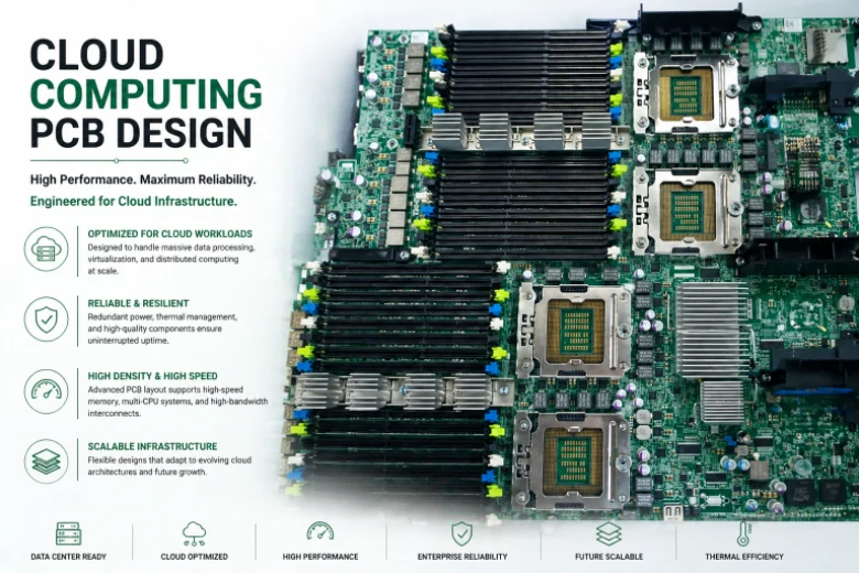
The global cloud infrastructure services market reached $330 billion in 2024 (Interaction Research), with AWS, Azure, Google Cloud, and regional providers deploying an estimated 3 million new servers annually — each containing PCBs manufactured to hyperscale quality standards where a 0.1% board failure rate translates to 3,000 simultaneous failures generating support tickets, SLA penalties, and replacement logistics at global scale. Cloud computing concentrates massive processing, storage, and networking capacity in hyperscale datacenters — delivering compute-as-a-service through hardware whose performance, power efficiency, and reliability are determined at the PCB level.
The economics of cloud hardware are fundamentally different from enterprise computing. A hyperscaler evaluating server motherboards doesn't ask "does this board work?" — they calculate total cost of ownership across 100,000-unit deployments where a 2W per-server power savings eliminates 200 kW of load ($175,000/year in electricity), a 0.05% reliability improvement avoids 50 field replacements per year ($25,000 in truck rolls), and a $3 per-board BOM reduction saves $300,000 per generation. Every PCB design decision carries fleet-scale financial consequences.
HILPCB manufactures cloud computing PCBs — delivering 16–28 layer server boards at volumes exceeding 5,000 units per month with Cpk >1.33 impedance consistency — for server OEMs, storage vendors, and networking companies building the physical infrastructure of cloud computing worldwide.
Menu Navigation
- Cloud-Scale Economics at the Board Level
- Server Motherboard Signal Integrity: DDR5, PCIe Gen 5, and CXL
- NVMe Storage Controller and Platform Design
- 400G/800G Network Switch and NIC Manufacturing
- Power Efficiency and Thermal Design for Maximum Rack Density
- Volume Production and Supply Continuity
Cloud-Scale Economics at the Board Level
Cloud hardware purchasing decisions are made through rigorous TCO modeling across 3–5 year deployment cycles. The PCB is not evaluated as an isolated component — it is evaluated as a contributor to performance per watt, reliability per dollar, and manufacturing cost at scale. Our co-design engagement with cloud hardware OEMs optimizes across these TCO dimensions from initial stackup definition through production ramp.Cloud PCB Optimization Dimensions
- Performance per Watt: Maximum compute throughput per watt of total system power — driving signal integrity optimization (achieving full interface bandwidth without retransmission overhead), VRM efficiency engineering (>93% at typical load), and low-loss material selection that reduces PCB dielectric heating.
- Reliability at Fleet Scale: 5-year continuous MTBF targeting <0.1% annual board failure rate across 100,000-unit fleets — achieved through component derating (30% voltage, 20% temperature on electrolytics), solder joint qualification (2,500+ thermal cycles per IPC-9701), and incoming material verification preventing latent defects.
- Manufacturing Cost at Volume: BOM cost optimization through standardized passive component values (reducing unique part numbers by 30–40%), panel utilization maximization (15–20% material savings through optimized array layout), and DFM-driven design that achieves >95% first-pass SMT yield.
- Serviceability and Remote Management: Hot-swap capability for field-replaceable units, comprehensive BMC sensor arrays with Redfish API, and diagnostic LED indicators — reducing mean time to repair from hours to minutes and enabling headless datacenter operation.
Server Motherboard Signal Integrity: DDR5, PCIe Gen 5, and CXL
Cloud server motherboards carry the fastest commercial interfaces simultaneously: DDR5 at 4800–6400 MT/s across 8–12 channels, PCIe Gen 5 at 32 GT/s across 128+ lanes, CXL 2.0 for memory expansion and pooling, and UPI/GMI for multi-socket interconnect at 16–24 GT/s. Each interface has loss budgets leaving minimal margin for PCB contribution — and they all share the same 16–28 layer board construction, competing for optimal routing layers and reference plane resources.Server Signal Integrity Engineering
- DDR5 Routing at 5600+ MT/s: 40Ω single-ended impedance with ±1 mil byte lane matching and fly-by topology simulated for write-leveling timing margin at every supported DIMM population (1DPC and 2DPC). DDR5's on-DIMM voltage regulator requires additional power delivery routing absent from DDR4 designs — VR12.5 power rails routed alongside memory data buses with proper isolation.
- Multi-Socket Interconnect at 24 GT/s: UPI 2.0 (Intel) and GMI3/Infinity Fabric (AMD) links traversing 6–12 inches between processor sockets with insertion loss below 8 dB at 12 GHz — requiring low-loss laminates (Df < 0.004 at 10 GHz) and back-drilled vias with <8 mil stub on 16–28 layer constructions.
- CXL 2.0 Memory Expansion: CXL Type 3 memory expander interfaces sharing PCIe Gen 5 physical layer — routed alongside standard PCIe slots but requiring tighter jitter budget allocation because CXL's cache-coherency protocol is less tolerant of link-level retransmission latency than PCIe posted writes.
- Production Impedance Verification: TDR impedance measurement on test coupons from every production panel, with eye diagram compliance verified on first articles at DDR5 (5600 MT/s) and PCIe Gen 5 (32 GT/s) data rates using calibrated BERT instrumentation.
NVMe Storage Controller and Platform Design
Cloud storage infrastructure is built on NVMe SSDs aggregated behind PCIe switch ICs — the storage controller PCB routes 16–96 lanes of PCIe Gen 4/5 from switch ASIC to SFF-8639, E1.S, or E3.S drive connectors, with each lane requiring individual impedance control and loss verification. These boards are simultaneously high-speed digital designs (PCIe at 32 GT/s) and power management challenges (switch ICs dissipating 30–100W in constrained form factors).Storage Controller Board Design
- PCIe Fan-Out Routing: PCIe Gen 5 switch fan-out across 100–300 mm distances on multilayer constructions (14–20 layers) with low-loss laminate signal layers, back-drilled via transitions, and optimized connector launch geometry — maintaining channel loss within specification across all 16–96 lanes simultaneously.
- Mixed-Protocol Coexistence: Dedicated routing layers for PCIe (85Ω differential) and legacy SAS (100Ω differential) with continuous ground plane shielding between protocols — preventing crosstalk between 32 GT/s PCIe and 22.5 Gbps SAS signals that would cause bit errors in the storage data path.
- Controller Thermal Management: Storage switch ICs dissipating 50–100W in HHHL or FHFL card formats with thermal via arrays, heavy copper power planes (2–3 oz), and component placement optimized for constrained airflow — maintaining junction temperature below throttling threshold with 10°C margin under sustained random write workloads.
- Per-Lane Eye Verification: Eye diagram compliance measured on every PCIe lane during first-article inspection — because a single lane with marginal eye margin creates intermittent link retraining that degrades storage IOPS and tail latency, with the failure appearing as a storage performance problem rather than a PCB defect.
400G/800G Network Switch and NIC Manufacturing
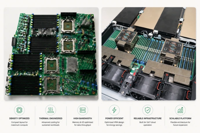
Cloud datacenters connect servers through 25G/100G/400G NICs and top-of-rack switches handling millions of packets per second. Next-generation 800G switches use 112G PAM4 SerDes (8×112G per port) with 224G PAM4 emerging — creating boards that are simultaneously ultra-high-speed digital and RF-grade analog design challenges. NIC PCBs carry network PHY ICs with 32–64 SerDes lanes, PCIe Gen 5 host interface, QSFP-DD/OSFP connector arrays, and sophisticated power delivery — all on boards measuring 150×200 mm.Network Board Manufacturing Capabilities
- 400G/800G Channel Design: 8×50G PAM4 (400G) or 8×112G PAM4 (800G) per port with insertion loss below 5 dB at 26.5 GHz (400G) or below 4 dB at 56 GHz (800G) — high-frequency laminates (Dk 3.0, Df < 0.002 at 28 GHz) on signal layers combined with standard FR-4 on power/ground layers for cost management in high-volume production.
- Switch ASIC BGA Escape: 5,000–7,000+ BGA pads with hundreds of 112G SerDes lanes requiring HDI PCB with sequential lamination on 24–36 layer constructions (capability up to 64 layers). Laser-drilled microvias at 0.075 mm with stacked via structures for complete ASIC escape within the package shadow — each SerDes lane individually impedance-tuned through via anti-pad optimization.
- NIC Power Delivery for Line-Rate Processing: Network PHY ICs drawing 25–50W from 0.75–1.0V core supplies with multi-phase regulation maintaining ±2% voltage under worst-case line-rate packet processing with full encryption — VRM transient response designed for the burst traffic patterns characteristic of datacenter east-west communication.
- EMI Pre-Compliance: Layout-integrated EMI assessment using near-field scanning — optimizing slot antenna radiation from plane gaps, connector shield grounding, and clock harmonic containment during board design rather than discovering compliance issues during FCC/CE/VCCI certification testing.
Power Efficiency and Thermal Design for Maximum Rack Density
Cloud datacenters are fundamentally power-constrained — every watt consumed by PCB losses (VRM inefficiency, resistive copper loss, dielectric heating) reduces available computation capacity. At fleet scale, PCB power efficiency improvements compound: a 2W per-server improvement across 100,000 servers eliminates 200 kW of IT load and 60–100 kW of proportional cooling load, saving $225,000+ annually.Efficiency and Thermal Optimization
- VRM Efficiency Profiling: Converter ICs selected and characterized at the specific load profile (not just peak efficiency) — targeting >93% at typical 50–70% load, >88% at 10% idle load, and >90% at 100% sustained load. Switching frequency, inductor selection, and gate drive strength optimized for the workload-weighted efficiency across the server's actual operating profile.
- IR Drop Engineering: 3.3V and 5V rails carrying 10–30A over 6–10 inches require copper weight calculated per rail and verified through DC IR drop simulation — often specifying selective 2–3 oz copper on high-current power layers within a standard 1 oz board construction to minimize resistive loss without increasing fabrication cost across all layers.
- 1U Airflow-Optimized Layout: Component placement creating unobstructed airflow channels from front intake to rear exhaust in 1U servers with 40–44 mm total height clearance. Tall components (VRM inductors, electrolytic capacitors) placed in downstream positions where they benefit from pre-cooled upstream airflow rather than creating blockages for downstream components.
- Thermal Derating for Datacenter Conditions: Component selection with temperature derating ensuring reliable operation at 35°C inlet air (ASHRAE A1 class) and 45°C (ASHRAE A3/A4 for free-cooling datacenters) — the growing adoption of free cooling in cloud datacenters increases ambient temperatures beyond what legacy server designs accommodate.
Volume Production and Supply Continuity
Cloud hardware production follows distinct patterns: 6–12 month design cycles driven by new processor generations, rapid production ramps from pilot to thousands per month within 8–12 weeks, sustained builds at peak volume for 18–24 months, and managed end-of-life with 12-month last-time-buy windows. Manufacturing agility and supply continuity determine whether an OEM meets datacenter buildout schedules — a 4-week delay in server delivery can postpone a $50M datacenter deployment by a full quarter.Production and Supply Chain Framework
- Rapid Prototyping: Initial development boards in 5–7 working days for hardware bring-up, BIOS development, and firmware validation — enabling hardware teams to begin system integration while production tooling is finalized.
- Pilot Production Qualification: 100–500 board runs establishing manufacturing process parameters, yield baselines, and test coverage metrics — pilot boards used for system qualification, regulatory certification, and customer sampling.
- Volume Ramp to 5,000+/Month: Automated SMT assembly with in-circuit test (ICT), boundary scan (JTAG), and functional verification — production line qualified for consistent quality at peak volume with real-time SPC monitoring on critical processes.
- Supply Continuity Planning: Buffer stock for 6+ week lead-time components, qualified second sources for all single-sourced ICs, and proactive end-of-life management with 18-month advance notification — protecting multi-year production programs from component supply disruptions.
Cloud Computing PCB FAQ
What are the key signal integrity challenges in cloud server motherboards?
Cloud server motherboards must simultaneously route high-speed interfaces like DDR5 (5600+ MT/s), PCIe Gen 5 (32 GT/s), and CXL 2.0. This requires tight impedance control, low-loss laminate materials, and advanced via structures (like back-drilling) to minimize insertion loss and preserve signal integrity across 16-28 layer board constructions.
How does PCB design impact datacenter power efficiency?
PCB power efficiency directly scales across thousands of servers. Designing for minimal IR drop using heavy copper power planes and optimizing Voltage Regulator Module (VRM) efficiency can save watts per server, translating to hundreds of kilowatts in savings across a hyperscale datacenter deployment.
Why is thermal management critical for NVMe storage controllers?
NVMe PCIe switch ICs can dissipate 50-100W within constrained form factors. Effective thermal via arrays, heavy copper planes for lateral heat spreading, and optimized component placement are required to maintain junction temperatures below throttling thresholds and ensure sustained storage IOPS.
Schedule a cloud hardware co-design review with our engineering team →