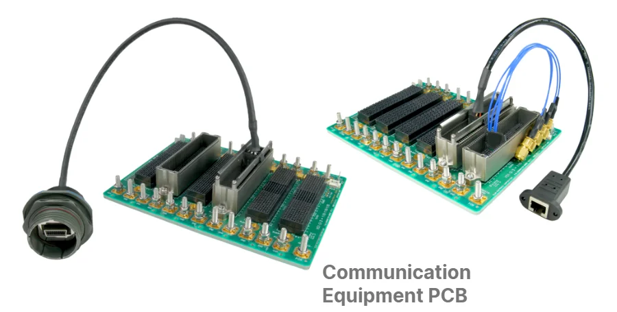
HILPCB specializes in communication equipment PCB manufacturing and assembly for telecommunications infrastructure, networking systems, and wireless devices. Our expertise covers cellular base stations, network routers, satellite communication equipment, and enterprise networking solutions requiring exceptional RF performance and environmental reliability.
Modern communication equipment demands advanced PCB designs integrating RF circuits, high-speed processors, and power management systems within ruggedized packages. We provide complete solutions from prototype development to high-volume production for telecom and networking applications.
Communication Equipment PCB Design Requirements
Communication equipment PCB design integrates multiple technologies including RF transceivers, digital signal processors, and power management circuits. The primary challenges involve maintaining signal integrity across high-frequency circuits while ensuring electromagnetic compatibility and thermal management.
Essential Design Elements:
• RF Circuit Integration: Multi-band transceivers supporting cellular, WiFi, and satellite frequencies with proper impedance matching and isolation between channels
• High-Speed Digital Processing: Advanced processors and FPGAs handling baseband processing with stringent timing requirements and signal integrity considerations
• Power Management: Sophisticated voltage regulation and power sequencing supporting diverse power requirements across communication subsystems
• Interface Controllers: Ethernet, USB, and specialized communication protocols enabling system interconnection and external device support
Communication equipment operates across frequencies from sub-GHz to millimeter-wave ranges. High-frequency PCB substrates maintain signal integrity while supporting complex impedance matching networks required for multi-band operation.
Environmental Considerations:
Telecom infrastructure equipment must operate reliably in harsh outdoor environments with temperature ranges from -40°C to +85°C. Environmental protection requires careful material selection, conformal coating compatibility, and enhanced assembly processes ensuring long-term reliability.
Manufacturing Processes for Telecom PCBs
Professional communication equipment PCB manufacturing employs specialized techniques and materials optimized for RF performance and environmental durability. Material selection directly impacts system reliability, signal integrity, and operational lifetime in field deployments.
Advanced Material Selection:
Rogers PCB materials including RO4003C and RO4350B provide stable dielectric properties essential for RF applications. These materials maintain consistent performance across temperature variations critical for outdoor telecom installations.
Heavy copper PCB constructions with copper weights up to 6 oz enable efficient power distribution for high-power amplifiers and switching circuits common in communication equipment.
Precision Manufacturing:
• Multi-Layer Constructions: Complex stackups with dedicated RF, digital, and power planes ensuring optimal signal integrity and electromagnetic isolation
• Controlled Impedance: Precision impedance control within ±5% tolerance for high-speed digital and RF interfaces
• Environmental Protection: Enhanced surface finishes and assembly processes ensuring reliable operation across extreme environmental conditions
• Quality Control: Comprehensive testing including impedance verification, signal integrity analysis, and environmental qualification
Quality systems ensure consistent manufacturing with full traceability throughout production processes meeting telecom industry reliability requirements.
Assembly Solutions for Network Equipment
Communication equipment PCB assembly requires precision techniques for complex mixed-signal designs integrating RF modules, processors, and power management circuits. Assembly processes must ensure optimal performance while maintaining long-term reliability.
Critical Assembly Requirements:
SMT assembly processes accommodate fine-pitch BGAs and RF modules with placement tolerances within ±20 μm. Specialized reflow profiles ensure reliable joint formation while protecting sensitive communication ICs.
Component Integration:
• Communication Modules: Cellular, WiFi, and Bluetooth modules supporting latest wireless standards with advanced antenna systems
• Network Processors: High-performance processors and controllers supporting gigabit and 10-gigabit networking functions
• Power Systems: Efficient voltage regulators and power management circuits optimized for communication equipment requirements
• Interface Circuits: Ethernet controllers, optical transceivers, and specialized communication interfaces
Environmental Hardening:
Outdoor equipment requires enhanced assembly processes including moisture protection, temperature cycling validation, and accelerated aging testing. High-TG PCB materials ensure mechanical stability under thermal stress.
Specialized handling procedures for communication modules include controlled storage environments and assembly within specified timeframes preventing degradation and ensuring field reliability.
Applications in Telecom and Networking
Communication equipment PCBs serve diverse applications from enterprise networking to carrier infrastructure, each requiring specific performance optimization and environmental considerations.
Cellular Infrastructure:
Base station equipment demands exceptional RF performance across multiple cellular bands with high-power amplifiers. Backplane PCB designs enable modular systems with hot-swappable components ensuring continuous operation.
Small cell systems require compact designs integrating multiple wireless protocols. HDI PCB construction enables miniaturization while maintaining RF performance.
Enterprise Networking:
Network switches and routers require high-density designs supporting hundreds of ports with advanced switching capabilities. Data center equipment prioritizes power efficiency and thermal management through optimized power delivery networks.
Wireless Communication:
Access points and wireless controllers integrate multiple radio systems with advanced MIMO and beamforming capabilities. Satellite communication equipment operates across C, X, Ku, and Ka bands requiring specialized RF design techniques.
Professional Manufacturing Services
HILPCB provides comprehensive communication equipment PCB services from design consultation through high-volume production. Our engineering expertise ensures optimal performance while maintaining cost-effectiveness and regulatory compliance.
Complete Service Portfolio:
• Design Support: RF and high-speed digital engineering optimization using advanced simulation tools and design verification
• Rapid Prototyping: Quick-turn prototypes with comprehensive testing and performance validation for accelerated development cycles
• Volume Manufacturing: Scalable production from prototypes to millions of units with consistent quality and delivery performance
• Testing and Certification: RF performance verification, environmental qualification, and regulatory compliance support
Quality and Compliance:
Turnkey assembly services include component sourcing, assembly, testing, and packaging with full supply chain management and traceability.
ISO 9001:2015 certification ensures consistent processes while environmental compliance including RoHS and REACH supports global market access. Pre-compliance testing minimizes regulatory risks and accelerates certification processes.
Our partnerships with accredited laboratories provide comprehensive certification support for FCC, CE, and carrier-specific requirements ensuring global deployment readiness.
Frequently Asked Questions About Communication Equipment PCB
Q: What makes communication equipment PCB design different from standard PCBs? A: Communication equipment PCBs require multi-band RF optimization, high-speed digital design, environmental hardening for outdoor deployment, and compliance with telecom standards. Critical considerations include electromagnetic compatibility, thermal management, and long-term reliability.
Q: Which materials are best for telecom infrastructure PCBs? A: Rogers high-frequency materials provide excellent RF performance for base stations and microwave equipment. Heavy copper substrates support high-power applications while high-TG materials ensure reliability in harsh environments.
Q: How do you ensure regulatory compliance for communication equipment? A: We implement comprehensive testing including RF performance verification, EMC validation, and environmental qualification. Pre-compliance testing and design optimization minimize regulatory risks while partnerships with accredited laboratories ensure certification support.
Q: What assembly capabilities do you provide for network equipment? A: Our services include precision SMT assembly for complex designs, environmental hardening processes, comprehensive testing, and system integration. We support both prototype and high-volume production with carrier-grade quality standards.
Q: Can you support both enterprise and carrier-grade equipment? A: Yes, we provide complete manufacturing services for all communication equipment categories including enterprise networking, cellular infrastructure, satellite systems, and wireless applications with appropriate optimization for each requirement.