
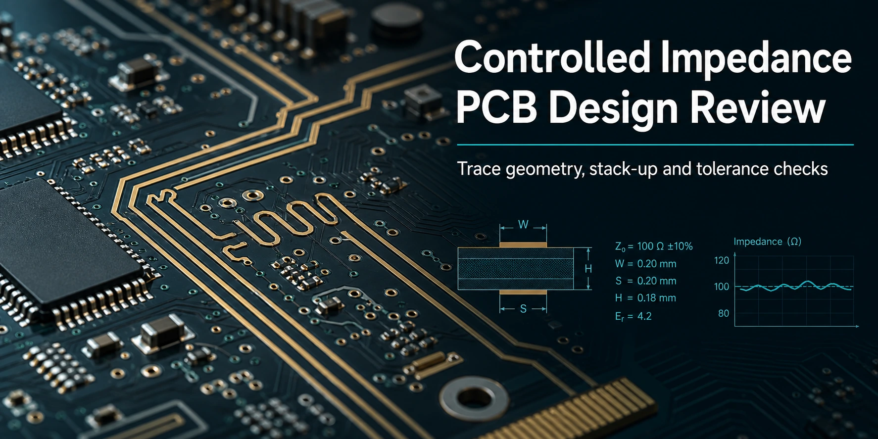
- Review controlled impedance as a foundational board-construction decision, not just as a passing note attached to a few nets. The stackup, reference planes, material weave, and validation posture must perfectly align before the fabrication package is frozen.
- Clearly separate the single-ended routing review from the differential routing review. While these net classes share the same board, they present entirely different challenges regarding coupling, return-path consistency, and layer transition behavior.
- Treat reference-plane continuity as an absolute approval gate. If critical nets cross plane splits, rely on ambiguous reference changes, or utilize poorly defined layer transitions, the board is fundamentally unready for fabrication release.
- Keep spread-glass (mechanically spread fiberglass), resin system, and copper-profile considerations tied directly to the actual stackup branch. Vague material language without exact stackup context is inadequate for a controlled-impedance review.
- Define coupon, Time-Domain Reflectometry (TDR), simulation, and prototype ownership before ordering the first build. A controlled-impedance release must state who confirms the stackup assumptions, how the prototype will be judged, and what the test coupons are supposed to prove.
A controlled impedance PCB design review is the final pre-release gate that confirms the board's construction can support the intended single-ended and differential net classes with stable references, realistic material assumptions, and a clear validation path. It is fundamentally a stackup-and-ownership review, not just a recipe for trace geometry.
Controlled impedance becomes a significant release risk when the board depends on trace behavior that simply cannot be left to generic manufacturing defaults. This engineering rigor does not strictly require the design to be an RF board, a backplane, or an extreme multilayer build. Ordinary digital and mixed-function boards frequently require a controlled-impedance review if specific nets (like USB, PCIe, DDR) depend on managed electromagnetic coupling, a predictable reference structure, and measured TDR validation.
The design-review question for quality and procurement teams is straightforward: Does the release package describe a board construction path that can be definitively evaluated, simulated, fabricated, and checked without relying on hidden or unstated assumptions?
This central question absorbs several older, fragmented topic patterns at once. Whether a team starts from "50 ohm PCB," "differential impedance PCB," "characteristic impedance PCB," "four-layer impedance control stackup," or "high-frequency layer coupling," the practical release burden remains identical. The board needs a coherent stackup, reference continuity, specified material direction, and a documented validation plan before fabrication data is frozen.
In This Guide
- What exactly does a controlled impedance PCB review approve before release?
- How do you structure the early release decisions for impedance control?
- How should you review single-ended vs differential nets without mixing the risks?
- Why must stackup and reference-plane continuity be locked before routing?
- How do material, spread-glass, and copper profile impact the impedance review?
- What should a controlled impedance validation and TDR testing plan look like?
- What are the most common review failures before fabrication release?
- What should be included in a controlled impedance PCB RFQ checklist?
- FAQ
- Next Steps
What exactly does a controlled impedance PCB review approve before release?
A controlled impedance review is frequently misunderstood as a narrow trace-geometry check. That perspective is too late and far too small in scope. Before fabrication release, the real approval is much broader: the engineering and quality team is approving a board construction path that can successfully carry the intended impedance-sensitive nets through fabrication and initial validation without relying on unspoken assumptions.
At the board level, this means explicitly confirming five linked items together:
First, the stackup branch must be explicit. A board containing impedance-sensitive nets is no longer just an ordinary routing exercise. Even when the layer count is moderate, the board has entered a planning tier where reference adjacency, layer-role assignment, and material direction heavily influence release quality. This is why a design that appears to be an otherwise standard Multilayer PCB may still require the intense review posture typically associated with a high-end High-Speed PCB.
Second, the review has to identify which nets actually belong in the controlled-impedance set. Teams often intuitively know that "USB," "clock," "SERDES," "camera," or "memory-side" nets matter, but the release file does not always state which nets are single-ended, which are differential, which transitions are sensitive, and which reference planes are expected to support them. If that classification remains vague, the board is not ready for approval, regardless of how polished the CAD layout looks.
Third, the board must have stable reference intent. Controlled impedance is not solely about the physical copper carrying the signal. It is equally about the surrounding electromagnetic field structure, especially the reference plane arrangement and how that arrangement behaves across layer changes, return-path interruptions, and routing escapes. When those paths are not deliberate, the nominal target impedance becomes meaningless because the actual board behavior will be dominated by inductive discontinuities that were never formally reviewed.
Fourth, the material direction has to fit the stackup. The available sources demand a planning posture in which spread-glass selection, resin system, copper profile, reference stackup, and verification are considered holistically rather than as isolated notes. This does not authorize publishing universal material claims or generic numeric promises; rather, it means the review must ask whether the stackup assumptions still make sense after laminate family, weave style, and copper roughness direction are considered in totality.
Fifth, validation ownership has to be assigned before fabrication. Controlled impedance cannot be approved as a pure design wish. The source set consistently connects impedance control to strict coupon-style and TDR-style verification postures. The exact tolerance, coverage, or acceptance criteria should not be generalized here, but the release package still needs to clearly state who owns the simulation assumptions, who owns the coupon testing posture, and what the prototype is expected to prove.
In practical design review, controlled impedance approval is therefore not a promise that every sensitive trace is absolutely flawless. It is a rigorous check that the board possesses an explicit construction logic. If a reviewer cannot answer the following questions quickly, the release is still weak:
- Which net classes are truly impedance-sensitive on this board?
- Which layers are intended to carry them, and exactly what references support those layers?
- Where are the sensitive transitions, neck-downs, or coupling changes located?
- Which material assumptions (Dk/Df, weave, copper roughness) were used when the stackup was calculated?
- How will the team correlate the theoretical stackup intent with the first-build physical validation?
When that construction logic is clear, the conversation can move productively into PCB Prototype planning or into a focused manufacturing review. When it is unclear, the project tends to drift into a dangerous "quote-first" behavior, where the board is treated as if factory feedback can replace fundamental design ownership. For controlled impedance, that is always the wrong order.
How do you structure the early release decisions for impedance control?
Controlled impedance review is most effective when it happens before layout polish becomes the main focus. Many teams wait until the board looks visually finished, then try to retroactively repair the stackup assumptions around it. That sequence usually causes immense friction because the routing has already adapted to a construction model that may not have been formally approved or calculated.
The safer, more predictable sequence is to treat controlled-impedance review as a core part of stackup release, not as a final note stamped on top of finished artwork. If the board already has internal documentation for layer assignment, target net classes, or a pre-layout field-solving pass, those records must be consolidated before supplier-facing discussion begins. If they do not exist yet, that absence is itself a critical review finding.
Controlled Impedance Release Risk Matrix
Use this matrix to understand what must be confirmed early in the release cycle to avoid downstream failures in TDR validation or signal integrity performance.
| Review Point | What to Confirm Early | Why It Matters for Production | Safe Release Posture |
|---|---|---|---|
| Net-Class Ownership | Identify precisely which nets are single-ended sensitive, which are differential, and which are ordinary bulk routing. | Impedance reviews fail fundamentally when critical nets are not clearly scoped or separated in the constraints. | Freeze the controlled-net list and required tolerances before release notes are finalized. |
| Reference-Plane Continuity | Confirm that critical layers have unbroken, stable reference plane support through their entire intended route. | Return-path uncertainty (inductance spikes) can invalidate otherwise perfectly calculated trace geometry assumptions. | Review plane changes, layer transitions, and slot-crossing risk before final layout signoff. |
| Stackup Branch | Decide whether the board is a baseline multilayer, signal-integrity-sensitive, HDI-sensitive, or a mixed hybrid branch. | Different density branches create vastly different review burdens and manufacturing capabilities. | Keep the impedance review intrinsically linked to the real physical board architecture and capability limit. |
| Material Direction | Check whether the laminate family, spread-glass direction, and copper profile thinking match the stackup intent. | Material choices directly affect field coupling assumptions, loss profiles, and TDR validation posture. | Treat material selection as a core part of stackup review, not merely a late purchasing detail. |
| Simulation Ownership | Confirm who produced or approved the stackup calculations and assumptions behind the controlled nets. | Unowned field-solver assumptions create avoidable release ambiguity when the factory asks questions. | Keep Dk/Df calculations and routing assumptions attached to named engineering owners. |
| Coupon and TDR Posture | Decide how the first build will correlate design intent with board-level TDR measurement. | Controlled impedance is a measured, provable workflow, not just a CAD software label. | Define the validation posture (test coupons, TDR criteria) before ordering prototypes. |
| Prototype Objective | State explicitly what the first build is expected to prove about the stackup and the SI performance. | One prototype cannot answer every open question cleanly; scope creep ruins validation. | Limit the prototype goal to a clear, measurable release hypothesis. |
How should you review single-ended vs differential nets without mixing the risks?
Single-ended and differential nets often get grouped together under one umbrella "impedance-control" label. While that is useful for scheduling, it is disastrous for engineering review. The board can carry both classes simultaneously, yet each class creates fundamentally different questions about coupling, field containment, transition behavior, and layout approval.
For single-ended nets (e.g., 50-ohm characteristic impedance), the review focus is predominantly on the relationship between the signal conductor and its reference environment. The critical question is whether the trace sees a stable reference structure along the exact path it is intended to use. Sensitive single-ended routing can fail review even when the trace width itself was calculated perfectly, simply because the return path changes under connectors, breakouts, voids, or layer transitions were not reviewed with equal care.
That is why single-ended controlled-impedance review must aggressively ask:
- Which layer does the net belong on, and why was that specific layer chosen?
- What plane is acting as the primary reference over the relevant route, and is it a solid ground?
- Do any route segments pass through plane interruptions, large anti-pad fields, or poorly defined layer transitions?
- Do local neck-down areas or breakout regions change the effective environment enough to deserve separate SI attention?
- Do the simulation assumptions reflect the actual routed environment (including adjacent copper fill) rather than an idealized straight trace in a vacuum?
Differential review (e.g., 90-ohm USB, 100-ohm Ethernet/PCIe) starts from a different framing. The question is not only whether each line sees a reference plane, but whether the pair maintains the intended coupling behavior, phase matching, and symmetry through the actual fabricated board structure. Pair behavior can be severely affected by unequal transitions, coupling changes through layer moves, breakout asymmetry, glass-weave sensitivity, and localized route edits that look minor in CAD but wildly alter the electromagnetic field relationship between the two conductors.
That means differential review must aggressively ask:
- Does the pair stay on layers and in environments strictly intended for coupled routing?
- Where do pair separation, escape behavior, or skew-sensitive structures change the coupling coefficient?
- Do connectors, vias, or package escapes disrupt pair symmetry in a way that introduces common-mode noise?
- Are the material and spread-glass assumptions consistent with the skew and timing sensitivity of the pair?
- Is first-build validation expected to prove geometry alone, or the broader stackup-and-coupling posture?
The crucial review discipline is to avoid flattening these two classes into one generic checklist item such as "impedance controlled traces." A board may be remarkably strong on single-ended reference continuity while still being critically weak on differential transition symmetry. It may also be perfectly acceptable for one class to receive stricter validation attention than the other, depending on what the prototype is supposed to prove.
This framing is especially useful when older discussions revolve around labels like "50 ohm PCB" or "100 ohm differential PCB." Those terms identify the goal, but they are not enough to approve a board. They say almost nothing about where the nets route, what references they use, how layer changes behave, or who is responsible for correlating the stackup assumptions with real fabricated coupons and TDR results.
Why must stackup and reference-plane continuity be locked before routing?
Teams often become more confident as routing congestion drops. That is reasonable for general manufacturability, but it can be highly misleading for controlled-impedance boards. A route that feels comfortable in layout software can still be functionally defective if the stackup and reference model underneath it were never stabilized.
The main reason is that controlled impedance is attached to physical board construction, not to copper artwork in isolation. The trace does not "carry" its impedance by itself. The effective behavior comes from conductor geometry interacting dynamically with plane spacing, dielectric structure, copper surface condition, and local return-path continuity. That is why stackup review has to happen before anyone treats the routing as settled.
Reference-plane continuity is the most common place where this principle breaks down. Designers may correctly identify the intended signal layer, but the review frequently stops there. In reality, the harder questions always appear after that point:
- Does the signal remain adjacent to a consistent, unbroken reference over the entire path that matters?
- Are the intended references fractured by power island boundaries, plane apertures, stitching strategy gaps, or connector escape voids?
- When the signal changes layers, is the return path transition (via stitching) as deliberate as the copper transition?
- Is the board relying on a generic routing convention that made sense on an older stackup but no longer matches the current release package?
This failure is usually physical, not theoretical. A team may calculate a perfectly clean USB 3.0 or PCIe differential pair, hold the width and spacing precisely, and still negligently let the route step across a ground-plane split while escaping a via field or working around a power island. At that instant, the return path stops behaving like the mathematical model that justified the impedance geometry. Return current is forced to detour around the slot, local loop inductance rises sharply, and the TDR will often show a massive inductive impedance peak at the crossing. That local discontinuity can create reflection, radiated EMI, and eye collapse even though the copper trace dimensions themselves were never the problem.
The lesson is blunt: controlled impedance is field management. If the reference plane is fractured, the formula is no longer describing the real structure.
These are not abstract signal integrity concerns. They are hard board-release questions because they determine whether the layout is using the identical construction model that the fabricator, the simulation owner, and the validation owner think they are releasing.
One practical release test is simple: if a reviewer were shown only the stackup, the critical layers, and the sensitive transitions, could that reviewer explain why the present routing strategy is acceptable? If not, the board likely still depends on informal knowledge rather than documented construction intent. For projects that are still converging on this layer architecture, routing the next step through a formal Multilayer PCB or High-Speed PCB discussion is usually more productive than requesting fabrication feedback against an under-defined release package.
How do material, spread-glass, and copper profile impact the impedance review?
Material discussion around controlled impedance often swings between two detrimental extremes. One extreme ignores materials completely and treats impedance as a pure layout geometry problem. The other extreme turns material names into marketing shorthand and assumes that blindly choosing a premium high-speed laminate automatically closes the review. Neither approach is adequate.
The most effective posture is one where spread-glass selection, resin system, copper profile, reference stackup, and verification planning are treated as intimately linked decisions. This does not mean every board requires exotic laminate discussions. It means the review must ask whether the chosen stackup still makes sense once physical material behavior is considered in the same frame.
Material vs Impedance Strategy Matrix
| Material Variable | Why It Matters for Impedance | Typical Engineering Strategy | Review Check |
|---|---|---|---|
| Resin System / Dk Stability | Standard FR-4 has a wider Dk tolerance and higher loss at frequency compared to engineered high-speed laminates. | Use standard laminates for <2 GHz edge rates; transition to high-speed materials (e.g., Megtron, Rogers) when insertion loss or Dk stability becomes critical. | Does the stackup calculation match the exact resin content (RC%) and Dk of the chosen prepreg/core? |
| Glass Weave (Spread Glass) | Standard glass weaves create microscopic resin-rich vs glass-rich areas, causing localized Dk variations and differential skew. | Use mechanically spread glass (e.g., 1067, 1078, 1086, 3313) or route off-angle to minimize fiber-weave effect on tight differential pairs. | Are differential pairs sensitive enough to timing skew to require spread glass or angled routing? |
| Copper Profile (Roughness) | Rough copper improves peel strength but increases skin-effect losses and effectively alters the perceived dielectric constant at high frequencies. | Move from standard copper to RTF (Reverse Treated Foil) or VLP/HVLP (Very Low Profile) copper for >5 GHz or long loss-sensitive traces. | Did the field solver account for surface roughness in the impedance and loss calculations? |
| Dielectric Thickness Tolerance | Impedance is extremely sensitive to dielectric thickness; prepreg pressing can cause thickness variations depending on copper density. | Demand strict press-out thickness calculations from the fabricator, especially for thin dielectrics in HDI boards. | Is the copper density on adjacent layers balanced enough to ensure uniform prepreg press-out? |
Spread-glass belongs in that frame because it matters critically when skew sensitivity and coupling consistency are part of the design burden. The key review question is not "Which glass style is universally best?" The safer question is "Does this board have enough edge-rate sensitivity that weave-related planning should be discussed together with the stackup?" If the answer is yes, the material conversation cannot be deferred until after the routing and validation assumptions are frozen.
Copper profile also firmly belongs in the review posture when impedance-sensitive nets are important. While this guide does not authorize broad numeric claims, it supports the fundamental principle that copper surface condition is one of the stackup assumptions that must not be detached from routing and validation language. High-frequency signals ride on the skin of the copper; rough copper increases resistance and loss, and must be modeled.
What should a controlled impedance validation and TDR testing plan look like?
Controlled impedance must be treated as a measured workflow. The supporting IPC sources repeatedly pair controlled-impedance posture with coupon-style and Time-Domain Reflectometry (TDR) verification language. The engineering consequence is absolute: a board should not be released with impedance-sensitive intent unless the project knows exactly who owns the validation path.
Ownership starts long before fabrication. Someone has to own the stackup assumptions that led to the routed geometry. That owner may be the design team, an SI engineer, a board architect, or a joint review group. What matters is that the assumptions are explicit. A release package that merely says "controlled impedance required" without naming the originating model is fragile because every later discussion becomes an exercise in guesswork.
Simulation ownership is part of this same chain. Final geometry should be simulated against the actual material, copper, finish, and specific fabricator context rather than relying on generic online templates alone. If the board depends on controlled impedance, the team must know whether the routing geometry came from a solved stackup assumption, an inherited corporate rule, a previous project, or just informal experience.
Coupon ownership comes next. The key release question is not the exact coupon pattern or acceptance threshold. The useful question is whether the board has a defined posture for correlating stackup intent with fabricated evidence. If the project expects first-build confidence on controlled-impedance nets, test coupon planning cannot be an afterthought. Factory impedance coupons are usually placed on the panel edges and represent the trace geometries of the board.
TDR posture follows naturally from that coupon posture. TDR is the method anchor for characteristic-impedance measurement. The right public statement is procedural: the board release should define whether TDR-style correlation is part of the validation workflow, what the acceptable tolerance is (typically ±10% or ±5%), and who interprets the result against the design assumptions.
Prototype review should connect these ownership layers into one simple question: What is the first build supposed to validate?
Safe, useful examples include:
- Confirming that the released stackup and routing posture are aligned enough to justify broader prototype learning.
- Checking that the controlled-net classification, layer assignment, and reference-plane model were correctly translated into the fabrication package.
- Correlating the expected board-construction model with actual coupon and TDR physical observations.
When a team asks for controlled-impedance support, the most useful intake package includes the stackup intent, controlled-net list, target layer usage, and validation expectations together. That is why an early handoff through an Impedance Calculator or DFM review can help structure the discussion, but it should remain a starting point rather than a substitute for the board's own release review.
What are the most common review failures before fabrication release?
Controlled-impedance boards usually fail review for structural reasons, not because the team forgot a buzzword. The same patterns appear repeatedly across otherwise different board types.
Turning impedance into a property of only the trace width. This encourages teams to spend review time on route appearance while ignoring the actual field structure. The result is a board that looks disciplined in CAD but still has weak reference continuity, ambiguous layer transitions, or unreviewed breakout environments that destroy signal integrity.
Mixing board families without reopening the stackup decision. A design may begin as an ordinary multilayer concept and slowly accumulate denser escapes, stricter differential paths, or stronger material sensitivity. If the board branch changes but the stackup review language does not, the release package becomes internally inconsistent. The file may still say "multilayer PCB," while the true burden has moved closer to a High-Speed PCB or HDI PCB planning problem.
Treating simulation as background noise rather than an owned input. Controlled-impedance geometry that came from an old project, a vendor note, or a rule-of-thumb may still be usable, but only if the present release explicitly accepts that origin. Unowned assumptions create the worst type of error because no one notices the gap until TDR measurement or bring-up fails.
Material drift. The route was designed against one stackup concept, then later discussions add different laminate expectations, spread-glass concerns, or copper-profile preferences without revisiting the layer plan. By the time the board reaches fabrication release, the material story and the geometry story no longer describe the same construction model.
What should be included in a controlled impedance PCB RFQ checklist?
A controlled impedance PCB quote will be significantly more accurate if the RFQ separates firm requirements from areas where the fabricator is expected to adjust geometries. If the manufacturer has to guess your stackup assumptions, the quote will either be padded for risk or priced too narrowly to be safe.
Use this checklist when submitting data to HILPCB or comparing PCB manufacturers.
1. Documentation and Files
- Full Data Package: Gerber/ODB++/IPC-2581, NC drill files, netlist.
- Fabrication Drawing: Must explicitly point to the impedance table.
- Impedance Table: A clear table listing target impedance, tolerance (e.g., ±10%), net type (single-ended or differential), target layer, and reference layers for each controlled net.
2. Stackup and Materials
- Material Specification: Explicitly name the required material family (e.g., IT-180A, Megtron 6, TU-872) or state "equivalent material meeting Dk X and Df Y at Z GHz".
- Reference Stackup: Provide a proposed layer stackup, but explicitly state whether the manufacturer is permitted to adjust trace widths/spacings or dielectric thicknesses to hit the impedance targets (this is highly recommended).
- Copper Weights: State starting and finished copper weights for all layers, as copper thickness directly impacts impedance.
3. Testing and Validation
- TDR Testing Requirement: Explicitly require Time-Domain Reflectometry (TDR) testing on the panel coupons.
- TDR Report Deliverable: Require a formal TDR test report to be shipped with the boards.
- Coupon Design: State whether the factory will generate the impedance test coupons on the panel edges (standard practice) or if they are embedded in the board design.
4. Advanced Geometry Rules (If Applicable)
- Glass Weave: Specify if spread glass or angled routing is required for specific layers.
- Surface Finish: State the finish (ENIG, Immersion Silver, etc.), as certain finishes (like thick gold or HASL) can impact high-frequency loss profiles.
- Etch Factor: Confirm if the manufacturer will apply their own etch compensation to your drawn trace widths to ensure the final etched width meets the impedance model.
FAQ
What is the difference between a controlled impedance PCB and a regular multilayer PCB?
A controlled impedance PCB is a board whose critical net classes depend on an intentional construction model (stackup, dielectric constant, trace geometry) to maintain a specific electrical environment. A regular multilayer PCB does not carry the same strict review burden for reference continuity, material-linked stackup assumptions, and TDR measurement ownership.
Should controlled impedance review happen only after routing is finished?
No. Review should begin when the stackup branch, critical net classes, and intended references are being frozen. Waiting until routing is finished often hides the fact that the board was built on assumptions that were never clearly approved.
Do single-ended and differential nets need the same review checklist?
No. Single-ended review is driven mainly by reference continuity and local environment stability. Differential review adds strict coupling and symmetry questions, especially through transitions, escapes, and material-sensitive areas.
Does a coupon or TDR note by itself prove the board is safe?
No. Coupon and TDR posture are part of the validation path, not a substitute for stackup review. TDR testing confirms the factory manufactured the board to the modeled geometry, but it does not prove the layout designer provided stable, unbroken reference planes.
Can controlled-impedance review be done on a four-layer board?
Yes. Controlled-impedance review is not limited to very high layer counts. A four-layer board heavily requires serious stackup and reference review if its critical nets (like USB or HDMI) depend on managed coupling, stable return paths, and measured validation.
When should a controlled-impedance board be escalated toward HDI review?
Escalation is worth discussing when routing density, via structure, breakout pressure, and impedance planning begin to interact tightly enough that the board is no longer behaving like an ordinary multilayer release. The trigger is architecture pressure, not a marketing label.
Next Steps
If the current design is already carrying HDI impedance complexity, unresolved plane-split risk, or uncertainty about whether the present stackup can hold impedance consistently in production, this is the point to stop treating the release package as mostly complete. Controlled-impedance programs usually fail expensively when stackup assumptions, return-path integrity, and coupon strategy stay implicit until after fabrication data is already frozen.
Send the stackup draft, target impedance requirements, and full Gerber package to [email protected], or upload the data through the Quote page. HILPCB's impedance engineering team will return DFM feedback within 24 hours. That review is meant to close the real pre-release risks: recalculating impedance with etch-factor compensation, checking reference-plane continuity and split-crossing exposure, and locking the most stable TDR coupon and validation path before production release.
- Impedance Calculator intake when the project needs a structured starting point for stackup and controlled-net discussion.
- HDI PCB review when density, via strategy, and impedance-sensitive escapes begin to overlap.
References
- IPC TM-650 test methods index
- IPC TM-650 2.5.5.7A, Characteristic Impedance of Lines on Printed Boards by TDR
- IPC TM-650 2.5.5.14, Measuring High-Frequency Signal Loss and Propagation on Printed Boards
- IPC board design standards overview