
Copper wrap is hole plating that continues around the edge of a plated hole and onto the surface. On a filled and capped via, planarization can thin or remove that copper before the cap is plated. Whether a particular section is acceptable depends on the hole construction and the standard edition, class, addenda and drawing requirements on the order.
Retaining wrap can affect surface copper, fine-line etching and inspection. Define the filled-hole locations and acceptance criteria with the fabricator before release, and use representative microsection evidence to check the agreed construction.
1. What Wrap Plating Is and Where It Applies
IPC-T-50 describes wrap plating as electrolytic hole plating extending from a plated via structure onto the surface. Filling, planarization and subsequent plating can change the copper at this transition. An unfilled hole has a different process history; determine its applicable requirements from the ordered construction and specification rather than assuming that every process produces an acceptable transition.
| Structure | Is a wrap requirement relevant? | Why |
|---|---|---|
| Unfilled plated through-hole | Check the ordered requirements and plating process | Its transition and processing differ from a filled, capped hole |
| Filled and capped via, including via-in-pad plated over | Identify the hole and check the applicable criterion | Fill and planarization can remove wrap before cap plating |
| Filled or covered via | Confirm fill, covering and any planarization steps | The construction and applicable criteria may differ from a capped via |
| Buried via in a sequential lamination | Identify the layer interface and fabrication sequence | Processing at an internal interface differs from final outer-surface processing |
| Laser microvia, including stacked or filled structures | Confirm the applicable microvia construction and criterion | Geometry and processing may differ from a through-hole |
| Tented or plugged via | Identify the actual treatment and any later processing | A treatment name alone does not establish the acceptance requirement |
List the relevant holes and treatment types in the fabrication data so the supplier can evaluate the actual process and acceptance requirements.
2. The Requirement in IPC-6012
IPC-6012 addresses rigid-board qualification and performance. The order must identify the applicable edition, class, addenda and any drawing-specific requirements. The applicable wrap criterion also depends on the feature and processing being assessed.
For historical context, the NASA Workmanship Standards Program presentation Printed Circuit Board Quality: Copper Wrap (2016, page 5) reports through-hole wrap thickness values of 5 µm for Class 2 and 12 µm for Class 3 and Class 3/DS, with Class 1 as agreed between user and supplier. Its diagram also identifies different values for microvias and buried vias. These are historical presentation values, not a substitute for the controlled document governing a current order.
Before disposition, ask the responsible quality authority to confirm the exact criterion, its measurement geometry, any required surface extension and how approved exceptions apply. Do not treat a surface extension length as a plating thickness. If the controlled text is unavailable, obtain the applicable requirement before judging conformity.
3. Why the Requirement Exists: Butt Joints and Knee Cracks
When wrap is removed before cap plating, the cap may meet the barrel at a flat interface across the hole opening, forming a butt joint. During thermal cycling, differences in expansion between copper, fill and laminate can stress interfaces and copper near the hole. The magnitude and location of stress depend on the materials, geometry, temperature history and construction.
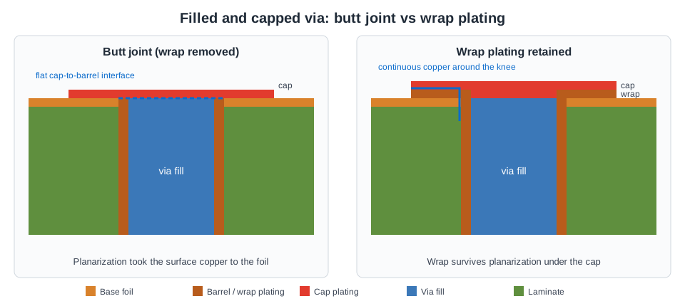
This conceptual illustration is not to scale and is not an acceptance reference for a microsection.
Two failure modes follow:
- Butt joint separation: the cap lifts from the barrel along the interface, creating an intermittent or permanent open.
- Knee crack: the barrel copper cracks at the corner where it turns onto the surface, especially when the plating there is thin.
Wrap copper provides a continuous path from the barrel around the corner and onto the surface beneath the cap. Expansion mismatch and board construction are factors to assess, but neither alone establishes the failure mode or lifetime of an actual board. Our via filling material guide covers fill selection.
4. The Trade-Off: Planarization, Surface Copper and Fine Lines
The wrap requirement is not just a plating target. It interacts with three things the board designer cares about.
Planarization variation. The 2016 NASA presentation states that planarization can vary wrap thickness by ±0.3 mil (about ±7.6 µm). In its separate panel assessment, the smallest observed within-panel thickness range was 0.2 mil and the largest was 0.94 mil; these are ranges across different panels, not the lowest and highest measurements on one panel. The presentation also reports spatial gradients. Neither number is a universal process tolerance.
An illustrative allowance. If a hypothetical process had a known one-sided reduction of 7.6 µm from its nominal starting value, then a 12 µm minimum would require at least 19.6 µm before that reduction in this simplified arithmetic: 12 + 7.6 = 19.6 µm. This does not establish an actual process target or guarantee acceptance; the real distribution, measurement uncertainty, feature and ordered criterion must be assessed with the fabricator.
Surface copper thickness. Wrap and subsequent plating can affect local surface copper, but finished thickness depends on the actual plating, patterning and planarization sequence. Ask the fabricator for the expected finished copper and etch feasibility at the relevant locations instead of adding nominal layer thicknesses as a general rule.
Fine-line etch capability. Thicker outer copper can limit the traces and spaces a fabricator can etch reliably. On a layer needing fine lines for BGA breakout, the copper required by the process may affect the manufacturing route or layer assignment. Ask the fabricator how its plating and patterning sequence affects the finished geometry.
5. What the Reliability Evidence Says
The same NASA study (NASA Workmanship Standards Program, "Printed Circuit Board Quality: Copper Wrap", 2016) tested through-hole coupons built with three controlled wrap conditions, 0 mil (no wrap), 0.2 mil and 0.5 mil, using interconnect stress testing (IST) and thermal cycling, followed by failure analysis and finite-element modeling.
| Finding | What it implies |
|---|---|
| Coupons with 0.2 mil and 0.5 mil wrap showed no significant difference in IST life at the reported 90% confidence level | The experiment did not establish a life difference between these groups in this construction |
| Zero-wrap coupons had longer failure times in accelerated cycling | This result describes the tested coupons and conditions, not a general design recommendation |
| Failure analysis located cracks in the barrel, away from the wrap | The observed failure location does not establish the cause or ranking of every contributing factor |
| Modeling showed stress maxima inside the barrel, not at the wrap | Consistent with the test results |
| The study noted that strict wrap minimums can raise scrap rates and lead times | A reliability benefit has to be weighed against yield cost |
The IST test used 14-layer polyimide coupons, a 245 °C solder-simulation precondition and cycling to 210 °C. The finite-element model represented a particular filled through-hole and assumed ideal quality. The presentation notes limitations concerning fill materials and construction; neither the test nor the model qualifies a different via, material combination or operating environment.
Use these findings to frame a project-specific discussion, not to waive an ordered wrap criterion. Qualification of a different construction requires an agreed test plan and acceptance decision.
6. Specifying Wrap: Decisions by Situation
| Situation | Recommended wrap specification | Reason |
|---|---|---|
| Class 3 product with via-in-pad under BGAs | Specify the governing edition and drawing requirements; request the process and agreed microsection evidence | Acceptance depends on the actual order and construction |
| Filled vias and fine-line outer layers | Review the complete stackup, line and space, finished copper and process with the fabricator | Manufacturability and acceptance both need to be addressed |
| Class 2 product with via-in-pad | Identify the filled-hole treatment and applicable requirements | A class label alone does not describe the construction |
| Other plated-hole constructions | Identify the process and applicable acceptance documents | A different hole or sequence can require a different review |
| Space, defense or automotive program with an addendum | Follow the addendum and the program's flow-down | Contractual requirement |
The via-in-pad guide discusses the layout trade-offs. If a design cannot meet an ordered requirement, involve the customer and responsible quality authority before changing the drawing or acceptance criteria. A supplier agreement alone does not establish product qualification or authorization to waive a contractual requirement.
7. Inspecting Wrap in a Microsection
Wrap is verified on a metallographic cross-section through filled holes, normally on a coupon from the production panel (see our test coupon guide and microsection report guide).
| What to check | Acceptable | Red flag |
|---|---|---|
| Continuity | Identify the barrel-to-surface transition and compare it with the ordered criterion | A discontinuity or an interface that needs further evaluation |
| Wrap thickness | Measure at the location and by the method required by the order | Local thinning, uncertain section plane or an unclear measurement boundary |
| Wrap extension | Measure along the surface where the applicable criterion calls for it | A short or unclear extension that requires assessment |
| Cap plating | Check the specified cap geometry and applicable criteria | Possible voids or separation that require evaluation |
| Sampling location | Apply the agreed sampling plan and identify each coupon's location | A sample whose location or representation is unknown |
The NASA panel assessment found gradients in its samples; one section cannot establish the condition of every board or location. When wrap is critical, discuss sampling across relevant panel locations, section planes, traceability and reporting with the fabricator. The IPC Class 1, 2 and 3 comparison provides broader context for selecting a class.
8. RFQ Checklist
- State the IPC-6012 revision and class, plus any addendum.
- Identify filled holes by type: via-in-pad plated over, filled and covered, buried vias filled during lamination, and stacked microvias. Reference IPC-4761 types.
- Specify the fill material or the required properties, especially z-axis expansion.
- State the applicable wrap criterion and identify any contractually approved exceptions; confirm the measurement method and location.
- Give outer-layer line and space at the filled-via locations, so the fabricator can confirm the copper thickness the wrap produces is etchable.
- Agree on microsection evidence, including the sampled features, panel locations, measurement method, traceability and report.
For multilayer PCBs and HDI PCBs, send the drawing, stackup, filled-via list and required inspection records with a quote request. Agree on the feasible construction, acceptance criteria and evidence for the order before fabrication. For broader context, see our IPC-6012 overview.
FAQ
What is copper wrap plating?
It is hole plating that continues from inside a plated hole, around the corner of the hole, and onto the surface. On filled and capped vias it sits under the cap plating, so the barrel and the cap are joined through continuous copper instead of a flat butt joint.
What is the IPC-6012 minimum wrap thickness?
The applicable value depends on the ordered IPC-6012 edition, class, construction and any addenda. A 2016 NASA presentation reports historical through-hole values of 5 µm for Class 2 and 12 µm for Class 3 and Class 3/DS; check the controlled order requirements before using a value for acceptance.
Does every plated through-hole need wrap plating?
Do not assume that one criterion applies to every plated hole or that an unfilled hole is automatically acceptable. Identify the hole construction and processing, then check the applicable requirements on the order.
Why does wrap plating make fine lines harder?
Wrap and subsequent plating can affect the copper that must be patterned. Thicker copper can make fine traces and spaces harder to etch; the actual trade-off depends on the fabricator's process and finished geometry.
Is thicker wrap always more reliable?
Not necessarily. In one NASA study of specific through-hole coupons, the 0.2 mil and 0.5 mil groups did not show a significant IST life difference at the reported confidence level, and analyzed failures were in the barrel. That result does not determine the acceptable thickness or reliability of another construction.