
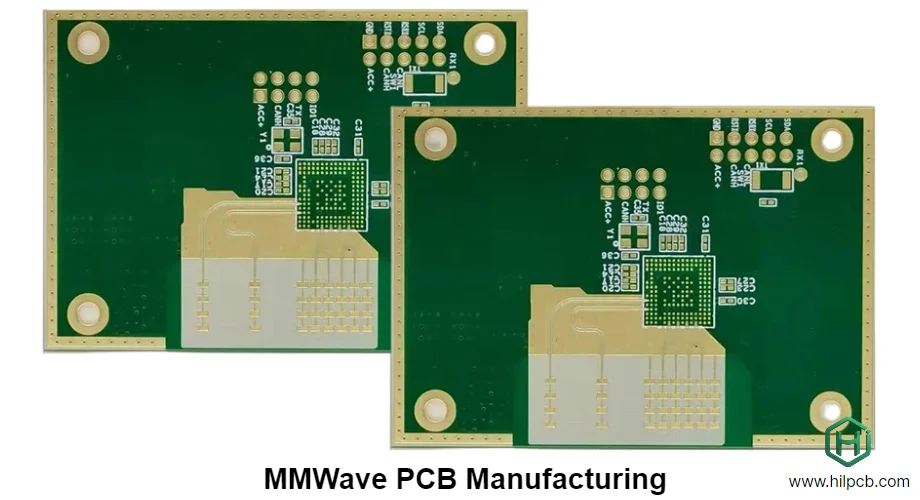
As 5G evolves toward 6G, communication systems are moving into higher mmWave bands, with data rates growing exponentially. This creates unprecedented challenges for PCB design, fabrication, and assembly. Signal attenuation, impedance discontinuities, thermal constraints, and yield quickly become make-or-break factors. In this context, a comprehensive and front-loaded DFM/DFT/DFA review is no longer optional—it’s the engine that turns a high-performance communication PCB from a design file into a shippable product. By tightly coupling design, manufacturing, and test, it identifies and resolves risks at the earliest stage—especially during NPI EVT/DVT/PVT.
DFM/DFT/DFA review: the foundation of 5G/6G PCB success
In the mmWave world, PCB is not just a carrier for components—it is part of the RF system. The traditional “design → build → test” linear workflow can’t keep up with high-frequency complexity. A unified DFM/DFT/DFA review closes the loop across three critical dimensions:
- DFM (Design for Manufacturability): can the PCB be built precisely, reliably, and cost-effectively? For 5G/6G, DFM focuses on material selection, stackup (especially hybrid lamination), fine line/space, via structures, and tolerance control.
- DFT (Design for Testability): can the PCB be tested effectively after manufacturing to validate function and performance? With dense BGA and leadless packages, traditional probing becomes impractical—so planning strategies such as Boundary-Scan/JTAG early in the design is critical.
- DFA (Design for Assembly): can components be assembled efficiently and reliably? This includes placement, pad design, stencil apertures, reflow profiling, and processes such as Low-void BGA reflow for high-value RF devices.
Integrating these in the design stage means you anticipate manufacturing tolerances, test coverage, and assembly yield. During NPI EVT/DVT/PVT, issues found via DFM/DFT/DFA review are vastly cheaper to fix—avoiding catastrophic rework or scrap in volume production.
Rogers/PTFE + FR-4 hybrid stackup: balancing cost and performance
To achieve ultra-low loss at mmWave frequencies, low Dk/Df materials such as Rogers and PTFE are often the first choice for RF layers. But they are expensive. A common optimization is a Hybrid Stack-up—using Rogers/PTFE only for RF layers and standard FR-4 for digital control and power layers. This approach is effective, but introduces major DFM challenges.
When should you choose a hybrid stackup?
When your design includes both high-speed RF signal paths and lower-speed digital/power circuits, hybrid lamination delivers the best value—keeping premium materials only where performance demands them.
DFM checklist for hybrid designs:
- CTE mismatch and reliability: PTFE typically has much higher CTE than FR-4. During lamination and thermal cycling, this mismatch creates mechanical stress at material interfaces and vias—driving risks like delamination and via cracking. DFM should evaluate stack symmetry and copper balance to manage stress.
- Press Cycle: Optimal temperature/pressure/time windows differ between materials. PTFE usually needs higher lamination temperature. Developing a unified Press Cycle that satisfies both materials is the core challenge and requires strong process know-how.
- Resin Flow and fill: During lamination, resin in FR-4 prepreg flows. It must be controlled to fully fill etched features in PTFE layers without over-flow that would degrade RF dielectric performance.
- Drilling and hole-wall treatment: PTFE is soft and tends to burr and smear; FR-4 is more brittle. One drilling recipe for both is difficult. PTFE also resists metallization, requiring specialized plasma/chemical treatment to ensure copper adhesion—very different from FR-4.
HILPCB has extensive experience with Rogers PCB and complex hybrid stackups, and uses tight process control plus strict DFM/DFT/DFA review to ensure both performance and reliability.
Material options comparison: all-RF vs. hybrid stackup
| Parameter | All Rogers/PTFE | Rogers/PTFE + FR-4 hybrid | All FR-4 |
|---|---|---|---|
| mmWave performance | Excellent (low Dk/Df) | Very good (RF layers protected) | Poor (higher loss) |
| Material cost | Very high | Medium | Low |
| Manufacturing complexity | High | Very high | Standard |
| Reliability risk | Low (uniform material) | High (CTE mismatch) | Low |
Copper roughness and weave effect: hidden killers of mmWave SI
At GHz—and even THz—frequencies, SI becomes extremely sensitive to microstructure. Two often-overlooked factors—Copper Roughness and Weave Effect—can become performance bottlenecks.
Copper Roughness
Because of skin effect, high-frequency current concentrates on the conductor surface. If the copper is rough, the effective current path becomes longer than a smooth surface, increasing conductor loss (insertion loss). In mmWave bands, this is especially pronounced.
- Standard ED copper: tooth-like profile; suitable for low-frequency circuits.
- Low-profile (LP) / very-low-profile (VLP) copper: smoother surfaces; standard choice for High-Speed PCB and high-frequency designs.
- Rolled Annealed copper: smoothest and best performance, but highest cost. In DFM review, select copper type based on operating frequency and loss budget.
Weave Effect
Dielectric layers typically use glass cloth plus resin. Glass (Dk ≈ 6) and resin (Dk ≈ 3) differ significantly, creating microscopic non-uniformity that drives local impedance variation—causing reflections and timing skew.
- Standard glass weave: larger resin windows; stronger Dk non-uniformity.
- Spread glass: more uniform dielectric; reduces weave effect substantially. DFM should recommend spread glass and suggest routing critical differential pairs with a slight angle (e.g., 5–10°) to average out Dk variation across multiple fiber bundles.
Via design and backdrilling: optimizing vertical interconnects
Vias are essential for layer-to-layer connectivity, but at high frequencies they are also major SI disruptors. The unused portion of a via—the stub—can resonate like an antenna at certain frequencies, causing severe reflections and insertion loss.
Backdrilling
Backdrill is a precision post-process that removes the via stub from the opposite side of the PCB.
- Benefits:
- Reduces deterministic jitter caused by stubs.
- Improves insertion loss and return loss to extend bandwidth.
- Reduces EMI/EMC radiation.
- DFM considerations:
- Stub length tolerance: depth control is critical; over-drill can damage signal layers, under-drill leaves excessive stub.
- Backdrill diameter: must exceed the original via diameter to fully clear the stub.
- Manufacturability: not all vias are suitable; spacing to adjacent routing/vias must be checked.
A strong Traceability/MES is essential for backdrilling—ensuring every specified via is backdrilled correctly, while recording process parameters for traceability.
Other via optimization strategies
Beyond backdrill, DFM should also cover:
- Ground via fencing: place ground vias around signal vias to provide a continuous return path and suppress crosstalk.
- Anti-pad optimization: tune clearance in reference planes to match target impedance and reduce capacitive effects.
- Remove non-functional pads: reduces parasitic capacitance and improves SI.
HILPCB manufacturing capabilities: precision interconnect technology
- ✔ Precision backdrilling: stub length controlled within 2mil (0.05mm), supporting 100Gbps+ signaling.
- ✔ HDI and microvias: supports Anylayer HDI; laser via diameter down to 50μm.
- ✔ Impedance control: tolerance to ±5%, verified 100% by TDR.
- ✔ Hybrid lamination expertise: extensive Rogers/Megtron/Teflon + FR-4 hybrid experience for high reliability and yield.
Manufacturability and testability: quality assurance from FAI to mass production
A well-designed DFM/DFT/DFA review proves its value across full quality control—from first article to volume.
First Article Inspection (FAI): for 5G/6G PCB, First Article Inspection (FAI) is far more than dimensional checks. It includes:
- TDR impedance test: validates key transmission lines against the design target.
- Microsection analysis: checks stackup, dielectric thickness, backdrill stub length, via wall copper thickness, etc.
- Material verification: confirms Dk/Df and other key parameters (e.g., via DSC). Passing First Article Inspection (FAI) is the first physical proof of manufacturability.
Traceability/MES: for complex hybrid lamination and backdrilling, consistency is everything. A robust Traceability/MES tracks material lots, lamination parameters, drill programs, and test data for every PCB—forming the foundation for quality assurance and rapid root-cause analysis.
DFT in practice: Boundary-Scan/JTAG: with shrinking pitch, physical probing becomes unrealistic. Boundary-Scan/JTAG (IEEE 1149.1) enables non-invasive, digital testing of connectivity (opens/shorts) on BGA/FPGA and similar devices. Ensuring chain integrity and accessibility during DFT review is key to high coverage.
DFA and assembly challenges: the final mile for mmWave performance
Even a perfect bare board is only half the story. Any assembly defect can invalidate the design and fabrication work. DFA review anticipates and prevents these risks.
Low-void BGA reflow: mmWave RFIC are highly sensitive to thermal and grounding performance. Voids in BGA joints degrade thermal conduction and can disturb impedance. Achieving Low-void BGA reflow usually requires:
- Stencil optimization: tune aperture size/shape to control paste release.
- High-quality solder paste: strong wetting and low-void formulation.
- Vacuum reflow: apply vacuum during liquidus to remove bubbles, driving voiding below 1%.
Warpage Control: hybrid stackups are more likely to warp during reflow due to CTE mismatch. Severe warpage causes opens/shorts on BGA. DFA should work with DFM—optimizing stack symmetry, copper balance, and assembly fixtures—keeping warpage within acceptable limits (typically <0.75%).
Placement and shielding: review RF component placement (decaps close to power pins, RF kept away from digital noise, and shielding cans when needed). PCB must reserve pads/space accordingly.
HILPCB offers one-stop PCB fabrication plus SMT assembly, ensuring seamless handoff from DFM to DFA with a fully optimized deliverable.
Assembly advantages: the last mile to mmWave performance
We know outstanding assembly is essential to unlock high-performance PCB potential. HILPCB assembly focuses on high-frequency, high-density challenges:
- Vacuum reflow: dedicated to Low-void BGA reflow to protect RFIC thermal and SI performance.
- 3D X-Ray and AOI: 100% inspection of BGA joints to prevent opens, shorts, and hidden defects.
- Fine-pitch placement: capability for 01005 and 0.35mm-pitch BGA precision placement.
- Functional test integration: combine Boundary-Scan/JTAG with customized functional test to ensure shipment-ready PCBA.
Conclusion
In the 5G/6G mmWave race, speed, performance, and reliability all matter. The key is a systems view from day one. A thorough DFM/DFT/DFA review is that systems view in action—not a static checklist, but a collaborative process spanning development.
By partnering early with an experienced manufacturer like HILPCB to align material choices, hybrid lamination, SI optimization, DFT strategy (such as Boundary-Scan/JTAG), and assembly risks (such as Low-void BGA reflow), you can avoid costly late-stage mistakes. From strict First Article Inspection (FAI) to end-to-end Traceability/MES, a complete DFM/DFT/DFA review is the strongest bridge from great design to high-performance, high-reliability 5G/6G products.
Common Questions
Why is a full DFM/DFT/DFA review especially important for 5G and 6G communication PCBs?
mmWave and high-speed communication products combine tight loss budgets, dense packaging, and strict production consistency requirements. A full review helps teams manage electrical, manufacturing, and assembly risks before they become expensive late-stage failures.
Why must materials and hybrid stackup strategy be reviewed so early?
Material behavior, copper roughness, and lamination structure directly affect insertion loss, impedance, and fabrication complexity. Once those choices are wrong, later routing or tuning changes usually cannot fully recover the design.
Why do DFT and assembly planning matter in high-frequency boards?
High-performance boards still need practical inspection, test access, and repeatable solder quality. Without coordinated DFT and DFA planning, the product may meet simulation targets but fail to scale into reliable manufacturing.
Why does early collaboration with a qualified manufacturer reduce risk?
An experienced manufacturer can flag realistic constraints in materials, backdrilling, BGA assembly, shielding, and test strategy before release. That shortens debug time and improves the odds of first-pass success.