

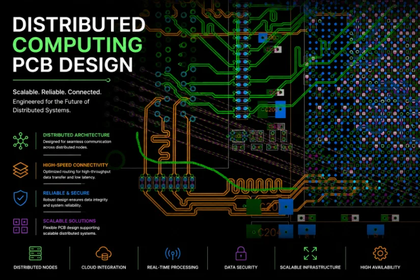
The global distributed computing market exceeded $5.8 billion in 2024, with blockchain infrastructure, content delivery networks, and scientific computing driving demand for consistent, fleet-scale PCB fabrication at volumes where manufacturing variation becomes a system-level performance problem. Distributed computing spreads workloads across tens to thousands of interconnected nodes — each running its own processor and memory, coordinating through high-speed network links using protocols (MPI, gRPC, libp2p, RAFT consensus) that are acutely sensitive to node-to-node performance variation. The Distributed Computing PCB in each node must deliver not just individual performance — it must deliver identical performance across every board in the fleet, because the slowest node in a distributed system becomes the bottleneck for the entire cluster.
This consistency requirement fundamentally changes the manufacturing quality paradigm. A standard server board is evaluated individually: does this board meet specification? A distributed computing board is evaluated statistically: does this production lot's performance distribution match every previous lot? A 3% impedance variation that passes individual board specifications but shifts node-to-node performance creates a stragglers problem in distributed workloads — a single slow node holding up a MapReduce barrier synchronization wastes thousands of CPU-seconds across the cluster with every synchronization event.
HILPCB has delivered distributed computing boards in lot sizes from 10 to 8,000 units with Cpk >1.33 impedance consistency and <0.5% variation in PDN impedance across production lots spanning 18 months — the population-level repeatability that fleet-scale distributed systems demand.
Menu Navigation
- Why Fleet Consistency Matters More Than Individual Specs
- Network Interconnect Design for 25G/100G RDMA
- Clock Synchronization and Memory Architecture
- Continuous-Operation Power and Thermal Engineering
- Statistical Manufacturing Quality at Fleet Scale
- From Pilot Run to 5,000-Board Production
Why Fleet Consistency Matters More Than Individual Specs
Every node in a distributed system must be interchangeable — operationally, any board must perform identically to any other. In a blockchain validation network, consensus latency depends on the slowest validator. In a CDN, content delivery SLA is set by the worst-performing edge node. In a scientific MapReduce cluster, barrier synchronization time is bounded by the last node to complete its partition.This means fabrication consistency beyond meeting individual board specifications is the primary quality metric. Impedance variation between boards shifts signal propagation velocity, creating node-to-node timing differences. Power delivery impedance variation creates node-to-node voltage droop profiles that cause different CPU boost clock behaviors. Thermal performance variation creates different throttling thresholds across the fleet.
Consistency-Critical Manufacturing Parameters
- Impedance Population Control: SPC tracking on every controlled impedance net across every production lot — not just individual board pass/fail, but population Cpk >1.33 with drift detection triggering process adjustment before any board leaves specification. Historical trend data maintained across lots enabling long-term consistency analysis.
- Copper Weight Uniformity: ±5% copper thickness uniformity across all layers within a panel and across panels within a lot — ensuring consistent power delivery impedance (copper weight directly determines plane resistance) and thermal performance (copper volume determines heat spreading capacity) from board to board.
- Assembly Process Consistency: SMT placement at ±25 μm accuracy with 100% post-placement AOI verifying uniform component alignment on impedance-sensitive pads — a 50 μm shift in a 0402 decoupling capacitor position changes its ESL contribution to the PDN by measurable amounts at fleet scale.
- Serialized Traceability: Each board serialized with laminate lot, copper foil batch, etching chemistry batch, reflow profile timestamp, and complete test result dataset — enabling root-cause analysis correlating field performance variations with specific manufacturing parameters across a deployed fleet of thousands.
Network Interconnect Design for 25G/100G RDMA
Network throughput and latency determine distributed system performance more directly than raw compute speed — a node with 20% more processing power but 10% higher network latency will slow the entire cluster on communication-intensive workloads. Modern distributed nodes use 25GbE or 100GbE with RDMA over Converged Ethernet (RoCE v2) for kernel-bypass networking that eliminates software stack overhead, reducing latency from 50 μs (kernel TCP) to <2 μs (hardware RDMA).The PCB network path from CPU PCIe root complex through traces, vias, and connector to the NIC PHY is the most performance-critical subsystem on any distributed computing board — and the subsystem most sensitive to fabrication variation between boards.
Network Interface Engineering
- 25G/100G SerDes Routing: Differential pairs at 25.78 Gbaud (NRZ for 25G) or 26.5625 Gbaud (PAM4 for 100G) with insertion loss below 6 dB at Nyquist frequency on inner stripline layers — 100Ω ±5% differential impedance with <1.5 mil intra-pair skew. High-speed PCB construction with mid-loss laminates (Df ≤ 0.005 at 12.5 GHz) sufficient for 25G and low-loss (Df ≤ 0.003) required for 100G.
- SFP28/QSFP28 Connector Layout: Connector-to-PHY routing following SFF-8402 (SFP28) and SFF-8665 (QSFP28) guidelines — maximum 130 mm trace length for 25G with via transitions limited to 2 per differential pair and via stub controlled to <8 mil through back-drilling.
- RDMA Latency Optimization: Deterministic latency through the hardware path requires elimination of impedance discontinuities and stub resonances that create inter-symbol interference (ISI) — ISI doesn't just degrade eye margin, it creates data-dependent latency variation (jitter) that directly increases 99th-percentile tail latency observed by the distributed application.
- Press-Fit Backplane Connectors: High-speed differential press-fit connectors requiring ±2 mil hole tolerances on multilayer boards with controlled impedance maintained through the entire connector transition zone — critical for distributed systems using backplane architectures with shared storage or network switching.

Clock Synchronization and Memory Architecture
Distributed systems require precise time coordination between nodes for event ordering, transaction sequencing, and synchronized data acquisition. Financial trading platforms require microsecond synchronization (PTP with hardware timestamping), industrial distributed control needs sub-millisecond (PTP or NTP), and scientific computing needs synchronized sampling across cluster nodes for time-correlated data analysis.The board's clock architecture — reference oscillator selection, clock distribution topology, and PTP hardware timestamping implementation — directly determines achievable synchronization accuracy.
Timing and Memory Subsystem Design
- IEEE 1588v2 Hardware Timestamping: PTP clock input routed on controlled-impedance traces with ±3 mil length matching between reference clock and timestamp latch — achieving <100 ns synchronization accuracy with hardware timestamping versus >1 ms with software-only NTP. For financial applications requiring <1 μs, dedicated PTP grandmaster clock input with OCXO holdover (±5 ppb) during GPS signal loss.
- Reference Oscillator Selection and Isolation: TCXO (±0.5 ppm, -40 to +85°C) for standard distributed computing, OCXO (±5 ppb) for financial and scientific applications requiring sub-microsecond synchronization. Thermally isolated mounting with >15 mm separation from heat-generating components and filtered power supply preventing switching noise from pulling oscillator frequency.
- DDR5 Memory Routing for Compute-Intensive Workloads: 4–8 channels DDR5 at 4800–5600 MT/s with fly-by topology, ±1 mil byte lane matching, and pre-layout simulation verifying write-leveling timing margins at all DIMM population configurations. Signal integrity validated for both 1DPC and 2DPC configurations on high-speed laminates with controlled Dk tolerance (±3%).
- Soldered LPDDR5 for Compact Nodes: For dense 1U distributed nodes using LPDDR5 at 6400 MT/s, HDI PCB with via-in-pad, 0.075 mm microvias, and 3/3 mil trace/space delivers the routing density required for 0.5 mm pitch package escape at ±15 μm registration accuracy.
Continuous-Operation Power and Thermal Engineering
Distributed nodes run 24/7/365 for 5–10 years under sustained computational load. Unlike edge devices with intermittent usage patterns or cloud servers with variable multi-tenant workloads, distributed computing nodes executing blockchain validation, CDN content processing, or scientific batch workloads maintain near-maximum power dissipation continuously — a thermal design providing only 5°C margin above sustained operating temperature will experience premature component aging, solder joint fatigue, and eventual field failure that impacts the entire distributed system.Sustained-Operation Design
- Heavy Copper Power Distribution: Multi-core processors drawing 125–350W TDP require multi-phase VRMs with heavy copper layers (2–4 oz internal) minimizing IR drop and resistive heating under sustained loads. Copper thickness calculated per rail — often specifying selective heavy copper (3 oz on processor Vcore layers, 1 oz on I/O layers) within a single board construction to balance power delivery capacity against signal routing requirements.
- Thermal Via Architecture: Filled and capped thermal vias (IPC-4761 Type VII) beneath processor and VRM power stages with 0.3 mm diameter at 0.8 mm pitch — conducting heat to bottom-side heatsinks without solder wicking during assembly. Via fill material (copper or thermally conductive epoxy) selected based on thermal conductivity requirements for the specific processor TDP.
- Material Selection for Decade Service: High-Tg FR-4 (Tg ≥ 175°C, Td ≥ 350°C) validated for long-term stability at sustained operating temperatures through 10,000-hour accelerated aging. CAF (conductive anodic filament) resistance validated through 1,000-hour 85°C/85%RH testing at rated voltage to prevent the electrochemical migration failures that kill boards after 3–4 years of continuous operation.
- Solder Joint Endurance: SAC305 joints validated through 3,000+ thermal cycles per IPC-9701 under continuous power conditions — exceeding standard 1,000-cycle qualification by 3× for always-on distributed infrastructure.
Statistical Manufacturing Quality at Fleet Scale
Manufacturing variation invisible in single-board production becomes system-impacting at distributed computing scale. A 3% impedance drift between production lots shifts CPU boost clock behavior. A 5% copper weight variation changes thermal resistance. A subtle reflow profile drift creates a population of boards with marginally weaker solder joints that fail 18 months before the rest of the fleet.Fleet-Scale Quality Control
- Real-Time SPC on Production Parameters: Automated SPC dashboards tracking impedance (TDR on every panel), copper weight (microsection every lot), drill registration (X-ray verification), etch factor, and solder paste volume — with Western Electric rules flagging process trends 2–3 lots before they would produce out-of-specification boards.
- Incoming Material Lot Verification: Dk/Df measurement on every incoming laminate lot using split-post dielectric resonator at 10 GHz — rejecting material lots whose dielectric properties would shift controlled impedance outside the design target, even if the material technically meets its own datasheet specification.
- Assembly Process Lock After Qualification: Reflow temperature profiles, pick-and-place programs, solder paste type and stencil design, and inspection criteria formally locked after pilot lot qualification — any change, including paste lot change, requires formal re-qualification preventing inadvertent process drift.
- Pilot Production Validation: 50–200 board pilot runs with complete electrical characterization, impedance population analysis, and accelerated thermal testing — validating manufacturing processes and quantifying yield before committing to full production volume.
From Pilot Run to 5,000-Board Production
Fleet-scale distributed computing requires testing strategies that catch systemic manufacturing issues before deployment — because a latent defect present in 1% of boards means 50 failing nodes in a 5,000-node cluster, each triggering workload rebalancing, data migration, and service degradation.Test Strategy and Production Scaling
- 100% Boundary Scan (JTAG): Verifies solder connection integrity on every BGA, QFN, and fine-pitch component — essential for high-density boards where visual inspection cannot access hidden joints.
- Signal Integrity Verification on First Articles: TDR impedance profiling and eye diagram measurement at actual data rates (25G NRZ, DDR5) on first-article boards — confirming production channel performance matches pre-layout simulation targets.
- 48–72 Hour Elevated-Temperature Burn-In: Powered operation at 55°C ambient (versus 35°C rated) under synthetic computational load stresses infant-mortality failure mechanisms — ensuring deployed boards are past the early failure region of the bathtub curve.
- Turnkey Fleet Production: Integrated procurement, fabrication, assembly, testing, burn-in, serialization, and logistics for fleet-scale deployments — maintaining consistent quality and traceability from 10-board pilot through 8,000-board production.
Distributed Computing PCB FAQ
Why is impedance consistency critical for distributed computing fleets?
In a distributed computing cluster, the slowest node dictates the overall performance. Variations in PCB impedance across a fleet can shift signal propagation velocities, creating node-to-node timing differences. Ensuring high statistical consistency (Cpk >1.33) guarantees identical performance across thousands of deployed boards.
What are the PCB requirements for RDMA network interconnects?
RDMA networks (like 25G/100G RoCE) demand ultra-low latency and minimal packet loss. The PCB must use low-loss laminates, precise differential pair routing (e.g., 100Ω ±5%), and back-drilled vias to eliminate stub resonances. This prevents inter-symbol interference (ISI) that causes jitter and latency spikes.
How do distributed node PCBs handle sustained thermal loads?
Unlike standard servers, distributed nodes often run near-maximum power 24/7. Their PCBs require heavy copper internal layers (2-4 oz) for lateral heat spreading, dense thermal via arrays beneath high-power components, and high-Tg materials to prevent long-term dielectric degradation under continuous thermal stress.
Get fleet-scale pricing for your distributed computing program →