
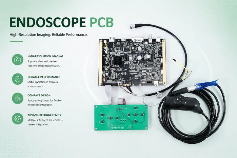
A gastroscope tip measures 9 mm in diameter. Inside that 9 mm circle: a CMOS image sensor capturing 1080p video at 60 fps, four to six white LEDs providing 5,000+ lux illumination, a lens assembly with 140° field of view, a biopsy channel for tissue sampling, air/water jets for lens cleaning, and articulation mechanism cables enabling ±210° tip deflection. The PCB hosting the image sensor and LED drivers fits within a 6 × 4 mm footprint, survives repeated autoclave sterilization at 134°C for 18 minutes, and must never raise the tip's outer surface temperature above 41°C — because it's touching the patient's esophageal or colonic mucosa.
Capsule endoscopes compress the constraint further — an 11 × 26 mm pill containing image sensor, LEDs, wireless transmitter, antenna, and battery, operating for 8–12 hours on two silver-oxide cells while transmitting images through abdominal tissue. Single-use disposable endoscopes add a cost constraint: the entire tip assembly including PCB must be economically discardable after one procedure.
HILPCB manufactures endoscope PCBs for medical device companies developing reusable scopes, capsule endoscopes, and disposable platforms using HDI, flex, and rigid-flex fabrication under ISO 13485 quality systems. Our manufacturing supports layer counts up to 64 for complex endoscope processor boards and video processing units.
Menu Navigation
- Tip-End PCB: Imaging in Sub-10mm Diameter
- LED Illumination and Patient Thermal Safety
- Rigid-Flex Through the Insertion Tube
- Image Processing in the Control Handle
- Capsule Endoscope: Complete System on One Board
- Sterilization, Biocompatibility, and Regulatory Path
Tip-End PCB: Imaging in Sub-10mm Diameter
The distal tip PCB is the most dimensionally constrained medical electronics board manufactured at volume. It mounts the CMOS image sensor (1/10" or 1/18" optical format — active area 1.0 × 1.0 mm or smaller) and provides all electrical connections to the signal cable running through the 1.5–2 meter insertion tube.
Tip PCB Design
- Non-Rectangular Board Geometry: The board shape follows the scope tip's internal cylindrical geometry — typically circular, 4–7 mm diameter, or D-shaped to accommodate the biopsy channel. CNC routing at ±0.05 mm on board outline. HILPCB fabricates custom-shaped HDI PCBs with smooth edge quality required for medical device assembly — no sharp burrs that could damage the insertion tube's internal lining during assembly.
- Bare-Die Sensor Mounting: Image sensors provided as unpackaged silicon dies — wire-bonded with 25 µm gold wire at 50–80 µm bond pad pitch, or flip-chip bonded using anisotropic conductive film (ACF) or gold stud bumps with thermocompression. The PCB's die attach area must provide <50 µm coplanarity for consistent optical alignment with the lens assembly. Epoxy underfill secures the die and protects bond wires from mechanical shock during scope insertion and articulation.
- Signal Routing in 4 mm Width: MIPI CSI-2 interface (1–2 lanes at 1.0–1.5 Gbps) or parallel CMOS output (8–10 bit at 40–80 MHz pixel clock) routed on a 2–4 layer HDI stack-up with 50/50 µm (2/2 mil) trace/space. Micro-vias (0.1 mm laser-drilled) for layer transitions within the constrained board area. MIPI lanes require 100 Ω differential impedance control even at these miniature dimensions — achievable through careful dielectric thickness specification and tight trace geometry control.
- Sensor Power Conditioning: The CMOS sensor requires 1.2 V core and 1.8 V I/O supplies with <5 mVrms ripple. Decoupling capacitors (0201 size — 0.6 × 0.3 mm) placed within 0.5 mm of the sensor's power pads. On a 4 mm wide board, these are among the largest components — space allocation for decoupling competes directly with signal routing channels.
- Electromagnetic Compatibility in the Tip: The LED driver's PWM switching, the CMOS sensor's pixel clock, and the MIPI transmitter's high-speed data all generate electromagnetic emissions within the confined tip space. Ground plane coverage ≥80% of the board area provides the primary EMI shield. LED driver traces routed on the opposite side of the board from sensor signal traces, with a ground plane between them.
LED Illumination and Patient Thermal Safety
Endoscope illumination uses four to six white LEDs at the tip, consuming 50–200 mW total optical power. IEC 60601-2-18 — the endoscope-specific safety standard — limits the tip's outer surface temperature to 41°C (2°C above body temperature at 39°C core). This thermal limit is the most stringent constraint on tip PCB design.
LED Thermal Engineering
- LED Driver on Tip PCB: Constant-current LED drivers (20–50 mA per LED) with PWM dimming capability. Current regulation accuracy ±5% prevents brightness variation across LEDs — visible as uneven illumination in the clinical image. Driver IC placement within 3 mm of the LEDs for short current loop paths. Multilayer tip boards with 2 oz copper internal planes provide thermal spreading within the sub-7 mm diameter constraint.
- Thermal Path to Scope Housing: LED junction heat must conduct through the PCB to the metal (stainless steel or titanium) tip housing — which serves as a heatsink cooled by tissue contact and irrigation fluid. Thermal vias (0.15–0.2 mm drill, 0.4 mm pitch) under each LED pad connect to internal copper planes. The thermal resistance from LED junction to housing outer surface must be below 50 °C/W to maintain compliance — verified by thermal simulation and validated by tip temperature measurement during qualification.
- Dynamic Thermal Management: NTC thermistor (0201 package) on the tip PCB provides real-time temperature feedback to the processor board through the insertion tube's signal cable. If tip temperature approaches 40°C, the processor dims the LEDs automatically — a hardware safety interlock verified independently from the main firmware control loop. The response time from temperature threshold detection to LED dimming must be <100 ms to prevent transient temperature overshoot.
- Medical-Grade LED Selection: LED packages for endoscope tips must not contain materials that degrade under repeated autoclave exposure. Glass-lens LEDs with gold wire bonds survive 1,000+ autoclave cycles. Epoxy-lens LEDs yellow and crack after 200–300 cycles — unacceptable for reusable endoscopes. LED spectral output must be stable across the 25–134°C temperature range — color temperature shifts during sterilization heating affect color reproduction in the clinical image.
Rigid-Flex Through the Insertion Tube
Traditional endoscopes route 20–40 individual signal wires through a 1–2 meter insertion tube — labor-intensive assembly, limited channel count, and susceptibility to wire fatigue at the articulation zone. Rigid-flex PCBs replace discrete wires with an integrated flex circuit strip.
Insertion Tube Flex Design
- Extended Flex Length: 1–2 meters of continuous flex circuit — among the longest flex spans manufactured for medical devices. Adhesiveless polyimide (12–25 µm base film) with ½ oz (17 µm) rolled annealed copper provides maximum flex life. HILPCB fabricates flex circuits up to 2 meters in single-piece construction — eliminating splice joints that create reliability weak points.
- Articulation Zone Flex Life: The scope's distal 50–80 mm articulates ±180°–±210° with a minimum bend radius of 20–30 mm. The flex circuit in this zone must survive 10,000+ full-deflection cycles (IPC-6013 Class 3 dynamic flex requirement) without copper fracture. Trace width ≥75 µm, trace spacing ≥75 µm, and no vias in the dynamic flex zone. Copper traces oriented perpendicular to the primary bend axis for maximum fatigue life.
- High-Speed Signal Through Long Flex: MIPI CSI-2 at 1.5 Gbps running through 1.5 meters of flex circuit. Insertion loss must stay within the MIPI receiver's equalization range — typically <6 dB at 750 MHz. Controlled impedance (100 Ω differential ±10%) maintained along the entire flex length. Polyimide's dielectric constant (Dk ≈ 3.4) and loss tangent (Df ≈ 0.005) are favorable for high-speed signaling — better than standard FR-4 — but the thin, narrow traces of the flex have higher per-unit-length resistance that increases conductor loss.
- Rigid-to-Flex Transitions: The flex connects to the tip PCB at the distal end and to the processor board at the proximal (handle) end. Each transition zone — where rigid and flex sections meet — sees the highest mechanical stress during scope manipulation. Stiffeners bonded to the flex at transition zones distribute stress. Copper traces fanned out gradually (not at right angles) from rigid pad pitch to flex trace pitch. HILPCB's rigid-flex manufacturing ensures controlled peel strength at the rigid-flex boundary exceeding 1.0 N/mm.
- Wire Count Reduction: A single flex strip carrying 20 differential pairs replaces 40+ discrete wires. Additional conductors for LED current, thermistor sense, and articulation motor drive share the same flex strip — reducing the insertion tube's outer diameter by 0.5–1.0 mm compared to wire bundle construction. This smaller diameter improves patient comfort and enables access to smaller anatomical passages.
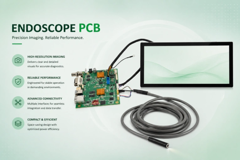
Image Processing in the Control Handle
The processor board — housed in the endoscope control handle or in an external video processor unit — converts raw sensor data to displayable HD/4K video, applies image enhancement algorithms (WLI, NBI, FICE for tissue characterization), and outputs to medical-grade surgical monitors.
Processor Board Design
- ISP and Video Processing: Image signal processor handling demosaicing, white balance, color correction, noise reduction, edge enhancement, and optional AI-assisted polyp or lesion detection. FPGA-based (Xilinx Zynq) or dedicated ISP SoC (Ambarella CV5). High-speed PCB construction with impedance control for MIPI input, HDMI/SDI output, and DDR4 memory interface.
- Video Output: HDMI 2.0 (1080p60 or 4K30) or SDI (3G-SDI for surgical environments) to medical-grade monitors. HDMI differential pairs at 85 Ω ±5%, matched to ±5 ps. SDI coaxial output driver with controlled impedance 75 Ω trace to the BNC connector.
- Image Recording: Video capture to SD card (SDIO interface) or network recording system (USB 3.0 or Gigabit Ethernet). For clinical documentation, each captured frame is tagged with patient ID, procedure timestamp, and scope serial number — the processor board's firmware manages this metadata, but the PCB must support the storage and network interfaces with adequate bandwidth.
- Control Interface: Scope control buttons (freeze, capture, white balance, illumination mode, zoom) interfaced through the flex cable from the control body. Debounced digital inputs with ESD protection. Foot pedal interface for hands-free capture during procedures — optically isolated inputs to prevent ground loops between the scope and external accessories.
Capsule Endoscope: Complete System on One Board
Wireless capsule endoscopes (PillCam, EndoCapsule, OMOM) contain the entire imaging system in an 11 × 26 mm pill — swallowed by the patient and transmitting images as it transits the gastrointestinal tract for 8–12 hours.
Capsule PCB Architecture
- Extreme Miniaturization: 8 × 8 mm PCB carrying CMOS sensor (typically 0.3–1 megapixel), 4 white LEDs, RF transmitter, antenna, battery management IC, and timing controller. 01005 passives mandatory. Bare-die sensor assembly with wire bonding or flip-chip. 3–4 layer HDI PCB with sequential build-up for complete routing in the constrained area.
- 30 mW Total Power Budget: Two silver-oxide button cells (SR44 or equivalent, 1.55 V each, ~80 mAh total capacity) must power 8+ hours of continuous capture-transmit operation at 2–6 frames per second. Total board power consumption must stay below 30 mW average — including LED drive, sensor, and RF transmitter. PCB leakage current through flux residue or solder mask moisture absorption must be below 0.5 µA — post-assembly ionic cleanliness verification is mandatory.
- RF Transmission Through Body Tissue: Capsule transmitters operate at 400–434 MHz (ISM band) or proprietary frequencies in the UHF range. Abdominal tissue attenuates RF signals by 30–50 dB. The PCB trace antenna (helical or loop, ∅8 mm) must be impedance-matched for in-body propagation — not free-space conditions. Antenna simulation using a tissue phantom model (permittivity ε ≈ 56, conductivity σ ≈ 1.0 S/m at 400 MHz for muscle tissue) is required for realistic link budget analysis.
- Biocompatible Total Encapsulation: The assembled PCBA is fully encapsulated in medical-grade optical epoxy (transparent for the LED/sensor window) inside a polycarbonate outer shell. All PCB materials — laminate, solder mask, solder alloy, flux residue — must pass ISO 10993-5 cytotoxicity testing as an assembled unit, since the encapsulant provides the biocompatibility barrier but must not react with any board material to produce toxic compounds.
Sterilization, Biocompatibility, and Regulatory Path
Medical Manufacturing Requirements
- Autoclave Compatibility (Reusable Scopes): 1,000+ steam autoclave cycles (134°C, 18 minutes, saturated steam). High-Tg laminates (Tg ≥ 180°C) with moisture absorption <0.1%. ENIG surface finish stable through repeated thermal shock. Solder joints — SAC305 lead-free with controlled intermetallic thickness — verified by microsection after 500 and 1,000 autoclave cycles during qualification.
- ISO 13485 Quality System: Full traceability from raw material lot through SMT assembly to final test. Design history file support for 510(k), CE MDR, and NMPA submissions. Change control per ISO 13485 Section 7.3.9 — any process modification (solder paste change, reflow profile update, laminate lot change) triggers customer notification before production proceeds.
- Disposable Endoscope Economics: Single-use scopes eliminate reprocessing risk (incomplete sterilization, cross-contamination) but require PCB costs low enough for single-procedure economics. Target: <$15 per tip assembly at 50,000+/year volume. HILPCB supports this through panel utilization optimization, simplified 2-layer tip designs where imaging requirements allow, simplified test strategies (go/no-go functional test rather than full parametric characterization), and turnkey assembly with component sourcing leverage.
- IEC 60601-2-18 Compliance: Endoscope-specific safety standard covering maximum tip temperature (41°C), leakage current limits, patient-applied part classification, and essential performance requirements. The PCB design must support compliance verification testing — including accessible test points for leakage current measurement and temperature sensor connections for tip temperature monitoring during type testing.
Start your endoscope PCB program — contact our medical miniaturization team →
Frequently Asked Questions
What is the smallest PCB diameter possible for a medical endoscope? HILPCB can manufacture endoscope tip PCBs as small as 4 mm in diameter, depending on the sensor size, LED count, and required routing channels. We use HDI and sequential build-up techniques to fit complex MIPI routing and power decoupling within this constrained geometry.
Why do endoscope PCBs need to survive 134°C autoclave cycles? Reusable medical instruments, including rigid endoscopes, must undergo saturated steam sterilization at 134°C to eliminate all pathogens between procedures. The PCB materials, including high-Tg laminates, solder mask, and ENIG surface finish, must withstand repeated thermal shock without delamination or performance degradation.
Can rigid-flex PCBs replace discrete wires in an endoscope insertion tube? Yes, rigid-flex PCBs can replace bundled discrete wires, which reduces assembly labor, minimizes the insertion tube diameter, and improves reliability in the articulation zone. Our extended flex manufacturing supports continuous lengths up to 2 meters without splice joints.
What is the maximum allowed tip temperature for an endoscope? According to IEC 60601-2-18, the outer surface of the endoscope tip must not exceed 41°C during continuous operation to prevent tissue damage. This requires careful thermal design on the PCB to conduct LED heat efficiently to the scope housing while utilizing dynamic dimming controls.