
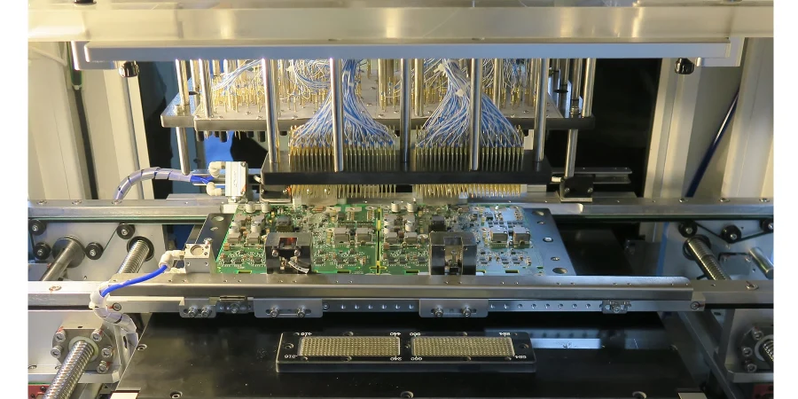
Driven by the AI and High-Performance Computing (HPC) wave, the design complexity of AI chip substrates and PCBs is growing exponentially. From Chiplet architectures to 2.5D/3D packaging, every technology node is pushing the limits of manufacturing and test. Yet beneath the spotlight of cutting-edge tech, one crucial (and often overlooked) link—Fixture design (ICT/FCT)—has become a key bottleneck that determines yield, reliability, and time-to-market. A well-designed test fixture is not only a tool for functional verification; it is also the “silent guardian” that connects design to mass production and helps ensure tens of thousands—or hundreds of thousands—of solder joints are defect-free.
As an engineer focused on thermal interfaces and tolerance control, I know that micron-level deviation can trigger thermal runaway or signal degradation at the system level. The same is true in ICT (In-Circuit Test) and FCT (Functional Test): fixture precision directly determines whether test results are valid. Poor probe contact, bad signal paths, or unintended mechanical stress can cause false failures (scrapping good boards) or, worse, allow latent defects into the field. This article dives into the core challenges and solutions of Fixture design (ICT/FCT) in the AI-chip era, and explains why it has become a critical lever for complex PCBA quality. Highleap PCB Factory (HILPCB) not only manufactures advanced IC Substrate PCB, but also deeply understands the role of test across the value chain—and builds manufacturing services that integrate strong test strategies.
What are ICT and FCT test fixtures, and why do they matter?
Before going into the design details, let’s clarify what ICT and FCT are and how they function in electronics manufacturing. They are two key quality gates on a PCBA (Printed Circuit Board Assembly) production line.
- In-Circuit Test (ICT): ICT focuses on manufacturing defects. Using a “Bed-of-Nails” fixture filled with probes (Pogo Pins), it contacts predefined test points on the PCB to check component parameters (resistance/capacitance/inductance values), detect opens/shorts on solder joints, and verify correct component installation. ICT is fast and highly diagnostic, and is an important method for ensuring SMT assembly quality.
- Functional Test (FCT): FCT simulates the real operating environment and verifies whether the PCBA works as a complete system as intended. It usually runs after ICT. The fixture applies stimuli (voltage, data streams, etc.) and measures outputs against expected behavior. FCT validates system-level function rather than individual components.
The core purpose of Fixture design (ICT/FCT) is to provide a stable, reliable, repeatable mechanical and electrical interface for both tests. A strong fixture design should achieve:
- Precise positioning: Secure the PCBA accurately so thousands of probes land on tiny test pads correctly.
- Reliable contact: Apply the right downforce so probes form stable, low-impedance electrical contact and avoid contact-related test variation.
- Signal integrity: For high-speed tests, internal fixture routing requires careful impedance control to avoid reflections and attenuation that corrupt results.
- Ease of operation and safety: Make loading/unloading easy and include poka-yoke features to prevent wrong or reversed insertion.
- Durability and maintainability: Fixtures must survive hundreds of thousands of cycles; they should be robust and allow easy replacement of worn probes.
For high-density, high-value AI substrates, the cost of a single mis-judgement is huge. Robust Fixture design (ICT/FCT) is therefore a foundation for high-quality, high-efficiency production.
Why do AI chip PCBs create unprecedented fixture design challenges?
Fixture design for traditional consumer electronics PCBs is relatively mature, but AI chip substrates and the complex PCBs they carry introduce new challenges driven by the core characteristics of AI hardware: extreme density, high speed, high power, and high complexity.
- Extreme high-density interconnect (HDI): AI substrates integrate tens of thousands to hundreds of thousands of interconnects, pushing test-point size and pitch to the limit (often < 0.4 mm). This demands micron-level precision in fixture machining, probe selection, and alignment systems. Tiny deformation or placement error can cause probe misses—or damage expensive PCBA.
- Severe high-speed SI requirements: AI systems are already in the era of PCIe 5.0/6.0 and HBM3e, with signal frequencies reaching tens of GHz. During FCT, test signals must pass through the fixture into the PCBA. If fixture routing is not carefully impedance-matched and shielded, the fixture itself becomes a noise source and attenuator, making it impossible to evaluate true performance accurately.
- Huge power and thermal demands: AI chips can consume hundreds of watts to over a kilowatt under full load. FCT must often simulate real load conditions, which generates significant heat on the PCBA. The fixture must not only provide electrical connectivity, but also integrate effective cooling (heatsinks, fans, or even liquid cooling modules) to avoid throttling or damage during test.
- Complex PI requirements: AI chips demand excellent transient response from the power network. An FCT fixture must carry large transient currents and measure small voltage droop precisely. The fixture PDN must have extremely low inductance and resistance; otherwise the test cannot reflect the real PDN performance.
- Widespread BGA and leadless packages: Many critical signals are hidden under BGA solder balls and are hard to probe via conventional test points. This increases reliance on technologies like Boundary Scan/JTAG, and Fixture design (ICT/FCT) must provide stable interfaces and control for those protocols.
These realities mean modern fixture design has long gone beyond “mechanical tooling”—it is a complex system engineering task combining precision mechanics, high-speed electrical design, thermal management, and software control.
Comparison: key fixture design parameters for ICT vs FCT
| Dimension | ICT fixture focus | FCT fixture focus |
|---|---|---|
| Test objective | Detect manufacturing defects (shorts, opens, wrong/missing parts). | Verify board-level functionality (simulate real operating conditions). |
| Probe density and type | High density; mainly standard probes contacting predefined test points. | Lower density, but may include high-speed coax probes, high-current probes, and connector probes. |
| Electrical design complexity | Lower; mostly point-to-point connections to tester channels. | Very high; requires impedance control, shielding, and decoupling, and may integrate load boards and signal-conditioning circuits. |
| Thermal management needs | Usually not needed because the PCBA is unpowered or powered at very low load. | Critical; must integrate active/passive cooling to control chip temperature. |
| Relation to DFM/DFT | Strong; relies on test-point placement/pitch defined in DFT. | Strong; depends on availability of functional interfaces, debug ports, and power access points. |
Precision mechanical design: the skeleton and soul of the fixture
The fixture’s mechanical structure is the foundation of everything. For high-value HDI PCB carrying expensive AI chips, any PCBA damage caused by fixture mechanics is unacceptable.
1. Material selection and structural rigidity
Fixture base plates and top plates are commonly made from ESD-safe synthetic stone, bakelite, or aluminum alloys. Material selection must balance rigidity, machinability, weight, and cost. For large, high-density AI motherboards, rigidity is critical—otherwise the fixture may deform under probe pressure and cause insufficient contact force in the center region. Finite Element Analysis (FEA) is often used to simulate and optimize the structure to keep deformation within limits at maximum load.
2. High-precision alignment system
Positioning accuracy directly determines test success. A typical approach is “three-point location” using two locating holes (one round, one slotted) plus multiple support posts. Tolerances of locating pins and the height consistency of supports must be tightly controlled (often within ±0.02 mm). For thin or flexible boards, vacuum hold-down or additional clamps may be required to keep the board flat.
3. Probe (Pogo Pin) selection and layout
Probes are the fixture’s “nerve endings”. Selecting probes requires considering:
- Tip geometry: For different surfaces (pads, vias, gold fingers), choose sharp, flat, crown, etc. to maximize stable contact.
- Spring force: Force must be high enough to break surface oxidation, but not so high that it damages the PCBA. Total downforce must be distributed evenly to avoid board bending.
- Current-carrying capability: PI tests may require high-current probes.
- High-frequency performance: High-speed tests may require dedicated coax probes with impedance matching beyond 40 GHz.
Probe layout is the core of Fixture design (ICT/FCT) and depends heavily on the test-point strategy defined during the early DFM/DFT/DFA review phase. A strong DFT design reserves sufficiently large and well-distributed test points for all critical nets.
Electrical design challenges in a GHz world
Once test signals enter the GHz domain, the fixture is no longer a simple collection of conductors—it becomes a complex high-frequency circuit system.
1. Impedance control and minimum path length
Every segment from the tester interface to the probe tip must be treated as a transmission line. Fixture wiring should use controlled-length coax cables or carefully calculated microstrip/stripline structures to match the DUT’s characteristic impedance (typically 50 Ω). Any impedance discontinuity (connectors, transitions) causes reflections and corrupts measurements. Signal paths should be as short and straight as possible.
2. Crosstalk and shielding
In dense routing, adjacent lines couple through electromagnetic fields, causing crosstalk. High-speed lines in the fixture must be spaced sufficiently or isolated with ground conductors. For highly sensitive signals (clocks, high-speed serial buses), use shielded coax cables with solid grounding. The fixture’s metal enclosure should also be grounded to form a Faraday cage and reduce external EMI.
3. Power Distribution Network (PDN) design
In FCT, the fixture must supply clean, stable power to the PCBA. Internal power paths should use wide, thick copper bars or multi-strand cables to reduce DC resistance and inductance. Near the PCBA power input, add ample decoupling capacitors on the fixture to absorb transient current noise when AI chips switch load, better emulating a real system-level supply.
Key reminders for high-speed fixture design
- ⚠️Impedance matching first: All high-speed signal paths inside the fixture must match the DUT strictly—this is the first principle of accurate testing.
- ⚠️The grounding network is core: Build a low-impedance, multi-point “star” or “mesh” grounding system to provide clean return paths for all signals.
- ⚠️Minimize path length: The shorter the distance, the lower the risk of attenuation, delay, and distortion. Place the test interface as close as possible to the probe region.
- ⚠️Isolate sensitive signals: Physically separate analog, digital, and power sections, and fully shield critical high-speed cables.
Why DFM/DFT/DFA must happen before fixture design
A design that is untestable—or difficult to test—cannot scale to mass production no matter how strong the functionality is. The success of Fixture design (ICT/FCT) depends heavily on early PCB design decisions. This is exactly why DFM (Design for Manufacturability), DFT (Design for Test), and DFA (Design for Assembly) reviews matter.
A comprehensive DFM/DFT/DFA review should resolve these questions early:
- Test-point coverage: Are test points reserved for all critical nets? Coverage directly determines ICT’s defect-detection capability.
- Test-point distribution and size: Are test points distributed evenly to avoid localized over-density? Do pad size and pitch meet the minimum requirements for fixture machining and probe selection?
- Keep-out areas: Is sufficient space reserved around board edges and tall components for clamps and locating pins?
- Component height data: Is accurate component height information provided so the fixture can avoid collisions with tall parts?
- Accessibility: Can all required interfaces/buttons/LED indicators still be accessed or driven after the PCBA is installed in the fixture?
Without early DFM/DFT/DFA review, fixture design becomes a compromise-heavy, risk-filled process—and may even leave some functions untestable. As a Turnkey PCBA provider, HILPCB treats this review as a key project kick-off step, ensuring the design is test- and production-ready from the source.
The fixture’s role in automated production lines
In modern electronics factories, testing is part of the automated flow. A PCBA coming off the SMT assembly line passes AOI (Automated Optical Inspection) and is then moved by conveyors or robots into ICT/FCT stations.
The fixture serves as the physical interface and must integrate seamlessly with automation (e.g., ATE—Automated Test Equipment). Pneumatic or motorized clamping systems replace manual operation, improving throughput and consistency. For PCBAs that require through-hole parts, FCT may occur after Selective wave soldering, and the fixture must be compatible with the final assembled form.
A well-designed automated test fixture shortens test cycle time, reduces labor dependence, and produces traceable test data—making it a key building block for Industry 4.0 manufacturing. HILPCB’s SMT Assembly service focuses not only on placement accuracy, but also on automated integration across the entire production flow, where Fixture design (ICT/FCT) plays an important role.
Where test fits in HILPCB’s one-stop Turnkey PCBA flow
Ensure design is manufacturable and testable
High-quality substrates and genuine components
Precision placement and reliable soldering
Custom fixtures and comprehensive testing
Product assembly and global logistics
Bed-of-nails ICT vs Flying probe test: how to choose?
When discussing fixture-based ICT, we should also discuss its main alternative—Flying probe test. Understanding the difference helps teams decide based on product characteristics and production stage.
Fixture-based ICT (bed-of-nails):
- Pros: Extremely fast once the fixture is built; test time is often 30–60 seconds per board. Ideal for high-volume production.
- Cons: High upfront cost. Each PCBA requires a dedicated fixture, typically 1–2 weeks to build. If the design changes frequently, fixture modifications are also expensive.
Flying probe test:
- Pros: No fixture required and extremely flexible. Programs can be generated directly from CAD data, making it ideal for prototypes and low volume, and for frequent design changes. Upfront cost is near zero.
- Cons: Very slow because probes must move point-to-point. Testing a complex PCBA can take tens of minutes or longer, making it unsuitable for high-volume production.
Selection strategy:
- Prototype and low-volume stage: Prefer Flying probe test to validate the design quickly and generate valuable feedback for later fixture design.
- Mid- to high-volume production: Investing in ICT and FCT fixtures is the inevitable choice. The efficiency and per-unit cost advantage quickly outweigh the one-time fixture cost.
In practice, many companies use a hybrid approach: Flying probe test during NPI, then switch to fixture-based testing after the design stabilizes for mass production.
Conclusion: treat test as an extension of design
In the precision world of AI hardware, Fixture design (ICT/FCT) has evolved from a simple “manufacturing tool” into a bridge connecting design validation to mass production. It is no longer the tail end of the process; it is a system engineering task that must be considered from day one. A successful fixture is a fusion of mechanical, electrical, thermal, and software engineering—and reflects a deep understanding of the DUT.
For AI products that target extreme performance and reliability, ignoring fixtures is like neglecting the foundation of a skyscraper. From early DFM/DFT/DFA review, to seamless integration with SMT assembly, to efficient, reliable test at scale—every link matters. Choosing a partner like HILPCB that provides integrated services from Turnkey PCBA through deep test-strategy integration means you’re not only getting a high-quality board—you’re gaining certainty in time-to-market. Ultimately, excellent Fixture design (ICT/FCT) helps ensure every shipped unit has passed rigorous verification and can deliver stable, efficient AI compute in the real world.
Common Questions
Why are ICT and FCT fixtures especially important for AI chip interconnect hardware?
Because AI interconnect boards combine dense packaging, fast interfaces, high current, and tight reliability requirements. A strong fixture strategy makes sure manufacturing defects and marginal performance issues are found before boards reach expensive system-level integration.
Why must signal integrity, power integrity, thermal behavior, and DUT protection be considered together?
AI hardware pushes multiple limits at once, so test accuracy depends on more than electrical contact alone. If the fixture disturbs SI, PI, or thermal conditions, or cannot protect the DUT from overstress, the test may create misleading results or even damage valuable hardware.
When should teams use flying probe testing instead of dedicated ICT or FCT fixtures?
Flying probe is usually the better choice when designs are still changing, volumes are low, and flexibility matters more than speed. Dedicated fixtures become worthwhile once the design is stable enough that throughput, repeatability, and lower per-unit test cost matter more.
Why should fixture planning start early in AI hardware development?
Early fixture planning feeds back into DFT rules, test-point strategy, connector access, and safe power-up methods. That reduces debug loops later and lowers risk when the product moves from prototype to pilot and mass production.