
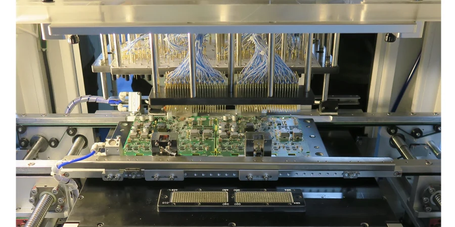
Fixture design (ICT/FCT): handling high power density and thermal challenges for power and cooling system PCBs
In modern power electronics, wide-bandgap devices such as SiC and GaN push power density and switching frequency to unprecedented levels. This raises strict requirements not only for PCB design, but also for validation—especially test-fixture engineering (Fixture design (ICT/FCT)). A well-designed fixture is essential to keep products like automotive-grade 48V to 12V conversion board and GaN power stage PCB design consistent and reliable in volume production. As your VRM/PDN design expert, this article explains how strong Fixture design (ICT/FCT) helps you manage high power density and thermal constraints while protecting performance.
From PDN impedance planning to precise transient validation and thermal management during test, every step is tied to the final SiC rectifier board quality. A poor fixture can introduce parasitics that cause false failures or even damage expensive prototypes through inadequate cooling. Understanding fixture fundamentals—and tying them back to early PCB design work (PDN modeling, decoupling strategy)—is the fastest path to a stable test ramp.
PDN target impedance: building a solid foundation for ICT/FCT
PDN Target Impedance is a key metric that defines the maximum impedance the power network can present to a dynamic load across frequency, keeping ripple within limits:
Z_target = (ΔV_ripple * V_out) / ΔI_transient
In design, engineers use simulation (e.g., Bode Plot analysis) to place decoupling capacitors so PDN impedance stays under target from DC to hundreds of MHz. This prep work matters directly to Fixture design (ICT/FCT)—a robust PDN is inherently more testable.
During ICT (In-Circuit Test), pogo pins contact test points to check soldering correctness and opens/shorts. If PDN design is weak and local impedance is high, even good components can read “bad” because Ground Bounce or supply noise distorts the test stimulus/measurement. For industrial-grade 48V to 12V conversion board, any test instability driven by PDN issues is unacceptable. Planning early (e.g., with an impedance calculator) is the first step toward high first-pass yield.
Decoupling strategy: design-to-test considerations
Decoupling networks achieve target impedance using capacitor arrays across values and packages, each covering specific noise bands:
- Bulk capacitors (electrolytic/polymer): supply large current at low frequency (kHz). Higher ESR/ESL.
- Mid-value MLCC (1–10 μF): main workhorse for mid-frequency (MHz) noise and fast load steps.
- Small-value MLCC (nF–pF): very low ESL and high SRF, suppressing high-frequency (>100 MHz) switching noise—especially important in GaN power stage PCB design.
In Fixture design (ICT/FCT), you must respect the existing decoupling loops. Pogo-pin landing points should avoid high-speed paths and critical decap current loops. Poor probe placement adds inductance, degrades decoupling, and can even trigger oscillation in FCT. For dense Multilayer PCB, reserve dedicated test pads near GND vias so test signals have the shortest return path.
Transient response and stability validation under high power density
Transient response describes how well a power system holds output voltage when load current changes abruptly (Load Transient). For automotive-grade 48V to 12V conversion board, load can step from near-zero to full load within microseconds; excessive overshoot/undershoot can damage downstream devices.
FCT is the primary method to validate transient behavior. Here, the key fixture goal is to reproduce realistic load steps—typically using integrated electronic loads capable of high dI/dt. Fixture design must ensure:
- Low-inductance connections: keep power/load paths between fixture and DUT short and wide to minimize parasitic inductance; otherwise fixture inductance can mask DUT transient behavior.
- Accurate measurement: use Kelvin (4-wire) sensing, sampling directly at the DUT output capacitor pins to remove cable drop error.
- Stability assessment: advanced FCT fixtures can integrate a network analyzer to inject small signals and measure Bode Plot, evaluating gain/phase margins across operating conditions—critical for validating compensation networks in GaN power stage PCB design.
Fixture SI: return paths and probe design
At high frequency, the fixture becomes part of the SI problem. Every probe and wire is a potential antenna or discontinuity. This is especially true when validating fast switching nodes on automotive-grade SiC rectifier board designs.
Return Path is the most commonly overlooked element. Signals enter the DUT via a probe, but they must return via a low-impedance path. In Fixture design (ICT/FCT), pair each signal probe (or group) with a nearby GND probe tied into the fixture GND plane, which must connect tightly to the DUT GND layer. This minimizes loop area, reducing inductance and noise susceptibility.
Probe selection and layout matter as well:
- Probe type: for high-frequency signals, use coaxial probes or low-inductance RF probes rather than standard spring probes.
- Test pad design: PCB test pads must be large enough for reliable contact, but not so large that they add excessive parasitic capacitance. Via-in-pad is a common way to create high-quality test points on dense boards.
- Ground grid: on a bed-of-nails fixture, GND probes should form a dense grid so every signal probe has a solid local reference.
Ignoring these details can cause a strong automotive-grade SiC rectifier board to fail test due to fixture-induced noise, hurting throughput and cost.
Fixture SI design checklist
- ✓ Shortest return path: place a nearby GND probe for each signal probe to minimize loop inductance.
- ✓ Low-inductance probes: for high-speed or high dI/dt nodes, use coax/RF probes.
- ✓ Impedance matching: for RF or high-speed digital tests, match probe/cable impedance to the DUT.
- ✓ Shielding and isolation: physically isolate and EMI-shield noisy power sections from sensitive analog/digital sections inside the fixture.
Thermal management as a critical factor in FCT
FCT often requires the DUT to run at full-load or overload conditions long enough to expose thermal weaknesses. For industrial-grade 48V to 12V conversion board, full-load dissipation can reach tens to hundreds of watts. Without effective cooling, power devices (MOSFET, SiC/GaN) can exceed safe junction limits, degrading performance or causing permanent damage.
Therefore, Fixture design (ICT/FCT) must include a properly engineered thermal system, such as:
- Custom heatsinks: designed around the DUT’s hot-device locations, with Thermal Pad or thermal grease interfaces.
- Forced air: fans integrated in the fixture to create controlled airflow across DUT and heatsinks.
- Liquid cooling: for extreme power density, integrate a Cold Plate solution.
- Temperature monitoring: add thermocouples or IR sensors at key points and automatically abort test on over-temperature to protect the DUT.
A strong FCT fixture keeps key components within spec under worst-case conditions. This directly impacts SiC rectifier board quality, since many electrical parameters (e.g., RDS(on)) are temperature dependent.
How manufacturing and process affect test yield
PCB manufacturing directly influences testability. As a leading PCB manufacturer, HILPCB understands design–manufacturing coupling. For boards like Heavy Copper PCB used in power products, we pay special attention to:
- Copper thickness uniformity: impacts pad flatness and probe contact stability.
- Solder mask accuracy: mask opening accuracy defines effective contact area; small or shifted openings cause poor contact.
- Warpage: thermal expansion during reflow and test can warp the board. Using High Tg PCB improves high-temperature dimensional stability. HILPCB controls production tightly to meet IPC warpage requirements so bed-of-nails fixtures compress evenly.
For complex GaN power stage PCB design, tight layouts and extreme sensitivity to parasitics require strict manufacturing tolerances. HILPCB capability helps translate design intent into hardware precisely, building a physical foundation for efficient and reliable testing.
HILPCB manufacturing capability: designed for testability
| Parameter | HILPCB standard | Impact on test |
|---|---|---|
| Warpage | ≤ 0.75% | Ensures reliable probe contact in bed-of-nails fixtures. |
| Minimum test pad size | ≥ 0.35mm | Provides a stable contact target for probes. |
| Solder mask bridge accuracy | ≥ 4 mil (0.1mm) | Prevents accidental shorts between dense test pads. |
| Copper thickness control | ±10% | Keeps current capacity and impedance consistency on power paths. |
ICT vs FCT: strategy synergy and fixture design differences
ICT and FCT complement each other, but their Fixture design (ICT/FCT) priorities are very different.
ICT fixture (bed-of-nails):
- Goal: detect manufacturing defects (opens, shorts, wrong parts, polarity, etc.).
- Design focus: maximize node coverage, so fixtures are dense with probes.
- Characteristics: typically unpowered or low safe voltage; fast; quickly locates manufacturing defects. Lower electrical-performance requirement, but high mechanical accuracy and probe-life requirements.
FCT fixture (functional):
- Goal: verify that the DUT functions to spec.
- Design focus: emulate real operating conditions—provide rated input power, apply loads, simulate inputs, and measure outputs (voltage, current, efficiency, ripple, etc.).
- Characteristics: powered DUT; more complex and time-consuming; very high requirements on fixture SI/PI and thermal capability.
For a complex automotive-grade SiC rectifier board, a typical flow is to run ICT first to screen out manufacturing defects, then send ICT-pass boards to FCT for full performance validation. This synergy maximizes efficiency and coverage. HILPCB Turnkey Assembly provides not only high-quality PCB fabrication and assembly, but also test-strategy planning and fixture development—an end-to-end solution from design through mass production.
Conclusion
Fixture design (ICT/FCT) is not “just mechanical.” It is a system engineering discipline that blends PDN, signal integrity, thermodynamics, and precision manufacturing. As power and cooling system PCBs move toward higher power density, higher efficiency, and higher reliability, test challenges become more visible. A scientific, well-engineered fixture is the bridge between a good PCB design and a high-quality final product.
From defining PDN target impedance to optimizing decoupling networks, accounting for manufacturing tolerances, and managing thermal effects during test—every decision impacts test yield and product reliability. With deep experience in power PCBs and advanced manufacturing, HILPCB delivers boards that are not only well-designed and well-built, but also “easy to test and verify,” helping you stand out in a competitive market.
Common Questions
Why are fixture requirements so demanding for power and cooling PCBs?
Because these boards often carry large current, switch quickly, and produce significant heat during test. The fixture must support safe power delivery, accurate measurement, and thermal stability without becoming the source of failure or measurement error.
Why do ICT and FCT fixtures have very different priorities on these products?
ICT focuses on manufacturing defects and node access, so probe density and repeatable contact matter most. FCT has to simulate real operating conditions, which means current handling, SI/PI behavior, thermal performance, and DUT protection become much more important.
Why must PDN target impedance and decoupling be considered in fixture design?
Because the fixture and the DUT form one temporary electrical system during test. If the fixture changes supply impedance or current paths too much, the measured ripple, transient response, and functional behavior may no longer represent the real design.
Why do thermal effects during testing matter so much for fixture accuracy?
As temperature rises, contact resistance, component behavior, and even mechanical alignment can shift. A fixture that ignores thermal loading may pass unstable hardware or fail good boards for the wrong reasons.