
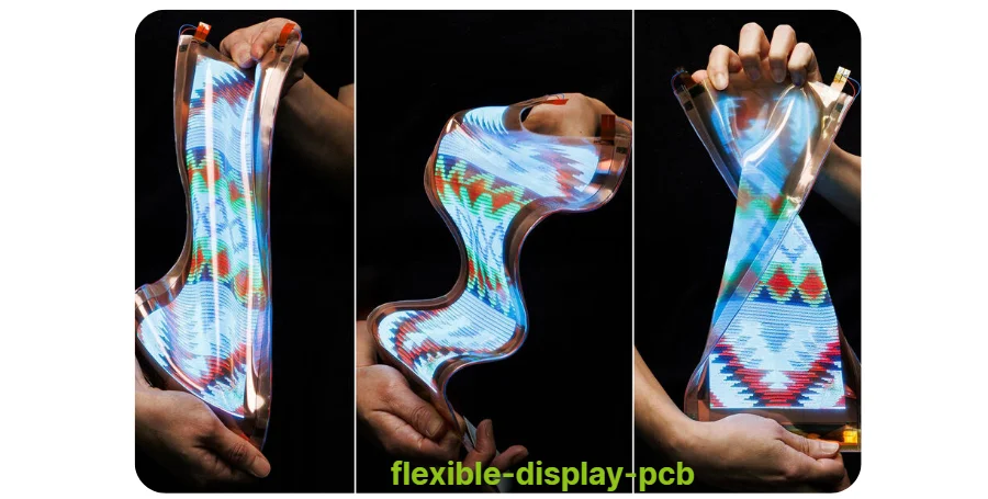
A flexible display PCB usually means a flexible interconnect, driver carrier or controller connection used with a display module. It is distinct from the OLED emissive layers, TFT backplane and display encapsulation. HILPCB's flex PCB, rigid-flex and assembly routes support the circuit-board portion of the design; panel fabrication and specialized chip-on-film or panel bonding need separate capability confirmation.
Start by defining which part moves. A tail folded once into a curved dashboard, an interconnect cycling through a phone hinge and the flexible panel itself have different mechanical requirements. Board construction alone does not determine display resolution, color accuracy or complete-screen endurance.
Flexible OLED PCB Design Guidelines
HILPCB provides mechanical simulation and signal-integrity engineering for the flexible interconnect, with bend geometry and the installed display link reviewed together. Separate electrical constraints from the bend mission, then review them together. IPC-2223 addresses flexible printed-board design; the applicable revision and customer requirements belong in the design package rather than being replaced by one universal radius.
Define the bend before the stackup:
- Motion: Static formed bend or repeated motion; inside radius, bend direction/angle, travel and any twist. Include the hinge or sliding mechanism drawing.
- Construction: Copper type/thickness, layer count, dielectric, adhesive, coverlay and shield/plane geometry. The copper's distance from the neutral axis affects strain; a nominal substrate thickness alone does not specify the complete flex stack.
- Transitions: Place stiffeners, connectors, vias and solder joints away from the active bend according to the approved drawing. Support the termination without creating a sharp strain concentration at the stiffener edge.
- Acceptance: Define electrical continuity, resistance change, visual damage and display/interface behavior during the specified motion and environmental exposure.
HILPCB's flex service lists 1–4 layers as standard and up to 8 after review, with 75/75 µm standard and 50/50 µm advanced trace/space options. PI/ED-copper and reviewed LCP/RA-copper constructions serve different needs. These are selectable routes; the finest geometry, most layers and tightest repeated bend are not automatically compatible.
The service also publishes dynamic-flex endurance options above 100,000 cycles and advanced targets above one million against a customer test plan. Its radius guidance is a screening input, not a guarantee for a finished foldable display. Confirm the exact stack, copper, bend fixture, radius, speed, temperature, sample count and failure criteria before adopting a cycle target.
For example, assume one complete open/close movement counts as one cycle, at 20 cycles per day for five 365-day years. The nominal mission is 20 × 365 × 5 = 36,500 cycles. This is a use assumption, not qualification evidence; the product owner must add the relevant margin, abnormal handling and environmental conditions. A claimed cycle count at a different radius or fixture is not an equivalent test.
For the display link, use the module and controller's actual interface requirements. Preserve return paths, connector launches, pair geometry where required, power drop and cable/flex length limits. Evaluate signal behavior in the installed and bent configurations; ordinary RF laminate is not automatically a flexible material.
Bendable Display PCB Materials Selection
Specify the complete flex region and the supported component areas separately.
- PI versus LCP: PI is the standard flex material route. LCP is an advanced option where its relevant electrical/moisture behavior fits the interface and construction; select the exact grade and verify the actual channel rather than buying it solely because a display is high resolution.
- Copper and coverlay: RA copper can be useful for repeated motion, but foil choice alone does not establish fatigue life. Review copper orientation, conductor shape, coverlay openings and adhesive flow with the bend geometry.
- Thickness and connector fit: The flex service lists standard finished thicknesses of 0.05–0.20 mm, with thicker builds available after review. Connector-contact thickness, stiffener tolerance, insertion depth and contact finish must match the selected connector drawing.
- Rigid or stiffened areas: A rigid-flex board can carry logic or power parts on rigid sections. A separate flex with PI/FR-4 stiffeners may reduce revision or service cost. Compare the complete interconnect and assembly cost, not just the bare-board area.
For manufacturing, release artwork/drill data, the layer stack, coverlay and stiffener drawings, finished outline and panel/handling requirements. HILPCB reviews the applicable imaging, hole/via, lamination and inspection route against those files. Do not assume that roll-to-roll processing, semi-additive sub-50 µm lines, embedded components or ultra-thin glass are standard features of a flex PCB order.
Impedance-controlled flex is available with ±10% and reviewed ±5% TDR-correlated routes. Agree the target, stackup, coupon and measurement condition, including whether the installed bend affects the acceptance method. A bare-board coupon does not qualify the complete display link.
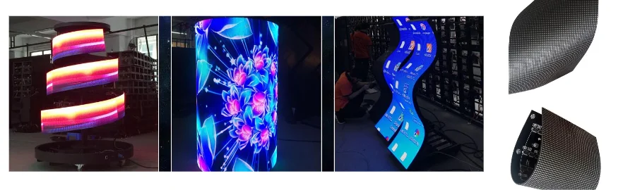
Flexible Screen Circuit Board Manufacturing Process
SMT assembly on flex needs support for printing, placement and reflow. Provide the panel/carrier concept, flat component areas and the final bend sequence so assembly does not load unsupported joints.
Component and connection choices:
- Display driver/controller: Identify whether the IC is a packaged SMT part, supplied as a pre-bonded display module, or requires a specialized chip-on-flex/film process. ACF bonding equipment and its thermal/pressure/pitch process are a separate scope from ordinary SMT; confirm the responsible supplier.
- Touch interface: Define the connector, pinout and electrical interface to the supplied touch panel. Fabricating transparent sensor layers is not implied by assembling its controller.
- Power parts: Check connector and trace voltage drop at the permitted brightness/channel state, startup and low supply. Keep hot or heavy components and their solder joints out of moving flex areas.
- Connectors: Use the specified ZIF or other connector's mating thickness, contact orientation, retention and insertion procedure. "Zero insertion force" does not remove latch, alignment or strain-relief requirements.
Select solder alloy and reflow limits from the laminate, adhesive, components and any attached display module. Lower-temperature solder is not universally required, and underfill or coating can change stiffness, stress and repairability. Keep adhesives, coatings and reinforcement within the approved areas and qualify their effect on the intended motion.
HILPCB's assembly service supports flex/rigid-flex builds after material and handling review, and can coordinate specialist panel or bonding providers where the quote identifies the supplier and scope. Agree SPI/AOI, selected X-ray, programming and functional checks for the actual package mix. Panel optical performance, specialized bonding and complete-screen bend qualification require their own test plans.
Foldable Display PCB Applications and Markets
The application determines whether the board is static, moving or replaceable. These are design examples, not claimed customer projects:
- Consumer electronics: A foldable phone may need a repeatedly moving hinge interconnect, while a watch may use a static curved tail. A rollable tablet or laptop must distinguish panel bending from motion of its controller connection. State the actual movement and enclosure constraints.
- Automotive displays and lighting: A curved dashboard or pillar-to-pillar display can use a fixed formed interconnect; it does not automatically need a dynamic-fold design. Review vehicle temperature/vibration, connector retention and cleaning exposure. A flexible lighting board is a separate LED power/thermal design, not OLED panel manufacturing.
- Medical and industrial: A patch display can require a small sensor/display interconnect and controlled contact materials. A machine panel may use a shaped but stationary connection. Mechanical and interface tests do not establish medical claims or complete-device safety.
- Aerospace: Weight and packaging may favor flex connections, with program-specific material, traceability, vibration and environmental acceptance. A lighter interconnect does not by itself qualify the display assembly.
Flexible Display PCB Testing and Quality Control
Use separate release checks for bare-board construction, assembly, motion and display operation.
Board and assembly acceptance: Specify electrical continuity/isolation, dimensions, coverlay/stiffener alignment, connector-contact geometry and agreed impedance coupons. For populated builds, define polarity, joint inspection, firmware and the power/interface test. Retain the approved revision and required lot or unit linkage.
Bend validation: Test the actual construction and mounting at the stated radius, travel, cycle rate and temperature. Monitor the required continuity/resistance or communication performance during motion, not only after the sample is flat again. Inspect the bend, stiffener and rigid-flex transitions. Passing accelerated conditions does not automatically establish a service lifetime without a justified correlation.
Environmental and optical validation: Agree temperature/humidity exposure, powered state, recovery and failure criteria. The display owner should define pixel/brightness/color or touch checks for the finished module. A PCB electrical pass does not prove display image quality, sealing or moisture-barrier performance.
Prototype and purchasing scope: HILPCB offers eligible 48-hour flex prototype builds and scalable volume planning after material, tooling and capacity review. Specialized procurement, protective packaging and global shipment can be coordinated for approved programs. Small-batch assembly supports development and pilot builds, while turnkey assembly includes the quoted sourcing/build scope. Provide exact connector/display part numbers and substitution rules; changing a tail, connector or module can alter thickness, pinout and bend behavior. Confirm the schedule, capacity and logistics in the quotation.
For a quote, send the fabrication/drill package, stackup, coverlay/stiffener and bend drawings, BOM/placement data, display interface and connector drawings. Include static/dynamic motion, radius, mission cycles, enclosure supports, environmental conditions, quantities and acceptance records. Identify who supplies the display module, specialized bonding, firmware and test fixture so HILPCB can price the actual flex/rigid-flex fabrication, sourcing, assembly and inspection work.
Frequently Asked Questions About Flexible Display PCB
What determines the minimum bend radius?
The complete flex thickness, copper layers/type, conductor position, coverlay/adhesive and motion all matter. A single-layer PI material name does not establish a universal 1 mm radius, and a static formed bend is different from repeated hinge motion. Submit the actual bend geometry and stackup for review and validation.
How can a repeated-flex endurance target be specified?
Define radius, angle/travel, speed, cycle count, temperature, mounting, sample count and electrical failure limits. HILPCB lists customer-plan-based dynamic test options, including advanced million-cycle targets, but these are not a guarantee for every stack or for the complete display. Use a representative assembly and retain the test conditions with the result.
What assembly challenges should be reviewed?
Flatness during printing/reflow, stiffener and connector fit, solder thermal limits, panel support and the bend sequence need review. Keep moving regions free of unsupported components and joints. Specialized ACF/chip-on-film bonding must be confirmed separately from ordinary SMT.
Can prototypes and production use the same construction?
They can when the released material, geometry, tooling and inspection route are available for both. Use the pilot to close handling, yield, mating and motion-test questions. Quote material availability, tooling, build quantities and test time explicitly; no universal 48-hour or million-unit capacity follows from a flex PCB service.
Who provides scalable tools for flexible display manufacturing?
PCB fabrication tooling, assembly carriers and bend-test fixtures serve different purposes from display-panel roll-to-roll machinery or chip-bonding tools. Identify the operation and responsible supplier first. Ask for the tooling and validation data needed for the quoted flex interconnect; confirm specialized panel or bonding processes separately.