
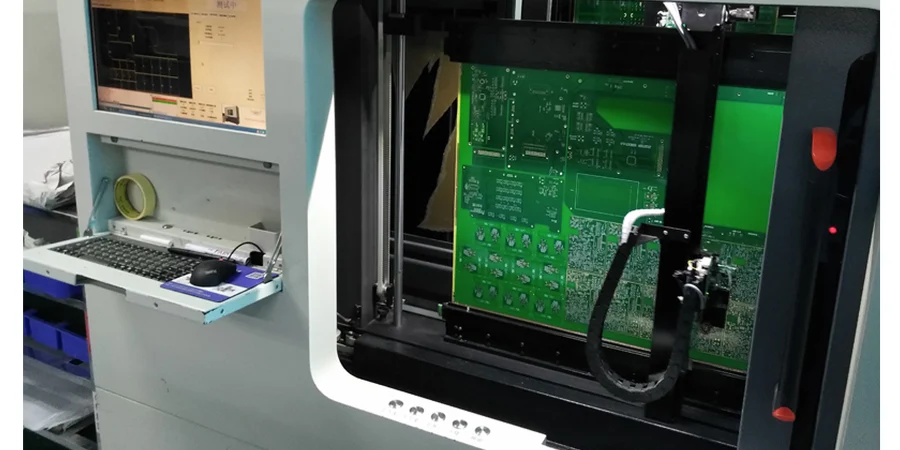
Flying probe testing is a programmable electrical test method that moves probes to accessible PCB or PCBA nodes without a product-specific bed-of-nails fixture. It is valuable for prototypes, high-mix production and changing revisions, but a standard continuity or component test does not prove controlled impedance, insertion loss, eye margin or bit-error performance on a high-speed channel.
Key Takeaways
- Define whether the test is for a bare board or an assembled PCBA; access, defect models and methods differ substantially.
- Standard flying probe commonly targets opens, shorts, isolation and selected component or connection checks, subject to equipment, access and circuit topology.
- A DC pass does not establish high-speed signal integrity. Use specified TDR, VNA, functional, compliance or BER evidence for the relevant channel requirement.
- Specialized robotic platforms can automate RF probes and external instruments, but that is a configured RF test cell—not an inherent capability of every flying probe tester.
- Measure net, node and defect coverage separately. “All tested nets passed” can hide inaccessible nets or untested fault classes.
- Provide design-intent netlist and intelligent product data in addition to manufacturing artwork so test engineering can detect data mismatches and preserve net names.
- Do not copy universal test-pad diameters or keepouts. Probe technology, angle, force, board support, component height and target finish determine access.
- Select flying probe, ICT, boundary scan, inspection and functional test as a complementary stack based on defects, volume and escape risk.
- Require a unit-linked report containing program revision, excluded coverage, limits, failures, retest and repair history.
Table of Contents
- What Does Flying Probe Test Actually Check?
- Bare-Board Flying Probe vs Assembled-Board Test
- Can Flying Probe Test Verify High-Speed Signal Integrity?
- Map Defects to the Right Test Method
- Flying Probe vs ICT, Boundary Scan and Functional Test
- Build and Validate the Test Program
- Design High-Density PCBs for Probe Access
- Protect High-Speed and Sensitive Nets During Test
- Choose Coverage, Throughput and Cost Deliberately
- Sequence Inspection and Electrical Tests
- Turn Results into Traceable Manufacturing Evidence
- Diagnose Common Flying Probe Failures
- Flying Probe Test RFQ Checklist
- Reference Standards and Responsibility Boundaries
- How HILPCB Supports Testable High-Speed Builds
- FAQ
- Conclusion
What Does Flying Probe Test Actually Check?
A flying probe system positions conductive probes on selected targets and applies a programmed measurement. For setup and program workflow, see the flying probe test tutorial. The useful capability comes from the complete configuration: mechanics, probe type, switching, sources, measurement instruments, software algorithms, guarding, cameras and any external equipment.
Depending on the machine and product, a program may include:
- bare-board continuity, shorts and isolation checks;
- resistance, capacitance, diode or polarity measurements on accessible assembled circuits;
- four-wire Kelvin measurements where contact arrangement and method support them;
- vectorless or capacitive techniques for some inaccessible device connections;
- powered measurements, programming, boundary scan, optical inspection or thermal checks on equipped platforms;
- automated RF or high-speed measurements only when appropriate probes, calibration structures and instruments are integrated.
Do not convert this menu into a blanket supplier claim. Circuit topology can mask an individual component, parallel paths can change a measured value, protection devices can limit test voltage, and a component body can block access. The approved program and coverage report—not the name of the machine—define what was tested.
Bare-Board Flying Probe vs Assembled-Board Test
The same mechanical idea serves two different quality gates.
| Aspect | Bare PCB electrical test | Assembled PCBA flying probe |
|---|---|---|
| Primary comparison | Fabricated copper against an approved netlist | Assembly against netlist, BOM and test model |
| Typical targets | Pads, vias and exposed copper before components | Accessible pads, vias, leads and test points around components |
| Main defects | Copper opens/shorts, isolation faults and some via/interconnect defects | Assembly opens/shorts, wrong or missing passives, polarity and selected connection faults |
| Access | Usually broad before assembly | Reduced by packages, shields, heatsinks, coatings and mechanics |
| Main limitation | Does not prove impedance, laminate quality or assembled function by default | Does not see every hidden joint or prove system performance by default |
Bare-board test should compare extracted manufacturing data with an independent design-intent netlist where available. Testing only a netlist extracted from the same faulty artwork can confirm that the manufactured board matches that artwork while missing the design-data error.
On an assembled board, distinguish one accessible point on a net from access to every meaningful node. A probe may confirm a rail exists without isolating which branch, solder joint or BGA connection is open.
Can Flying Probe Test Verify High-Speed Signal Integrity?
Standard flying probe tests are usually low-frequency or DC manufacturing screens. They can catch copper opens, shorts, gross resistance anomalies and selected component faults that would certainly damage a high-speed channel. They do not directly measure the channel's impedance profile, insertion loss, return loss, mode conversion, crosstalk, jitter, eye opening or BER.
Use requirement-specific methods:
- TDR/TDT for controlled-impedance profile, discontinuity location and propagation behavior under a defined fixture and calibration method;
- VNA measurements for frequency-domain insertion loss, return loss, coupling and mixed-mode S-parameters;
- oscilloscope or compliance testing for transmitter/receiver electrical requirements and eye or jitter metrics;
- functional traffic and BER testing for the implemented link under defined pattern, rate, equalization, channel and environmental conditions;
- coupon and material/process evidence for production control when product access is unsuitable.
Some current flying probe platforms can carry high-frequency probes and automate a VNA or TDR measurement. That can be powerful for repeatable production probing, but it needs a controlled launch, suitable probe geometry, calibration/de-embedding, stable contact force, reference structures and correlation with the accepted bench method. A standard pogo contact and resistance measurement cannot be renamed an RF test.
Map Defects to the Right Test Method
This matrix prevents the phrase “electrically tested” from becoming a substitute for explicit coverage.
| Risk or defect | Flying probe contribution | Complementary evidence | What a flying probe pass does not prove |
|---|---|---|---|
| Copper open or short | Direct continuity/isolation on accessible nets | Independent netlist comparison and failure localization | Impedance or intermittent behavior under stress |
| High-resistance via or connection | Kelvin or resistance screening when method and access support it | Microsection, current/load test or reliability evaluation | Via plating thickness or long-term life |
| Wrong passive value | In-circuit measurement where topology permits isolation/guarding | AOI, BOM traceability and functional test | Tolerance under every bias/frequency condition |
| Reversed diode or polarized component | Polarity/diode measurement on supported accessible circuits | AOI and functional test | Correct system behavior at operating stress |
| BGA solder open | Indirect access, vectorless or boundary scan on suitable designs | X-ray, boundary scan and functional test | Complete hidden-joint quality |
| Differential-pair copper defect | Opens/shorts and gross resistance mismatch | Differential TDR/VNA or qualified coupon | Differential impedance, skew, loss or mode conversion |
| Wrong stackup or dielectric | Little or no direct proof in standard test | Traveler/material records, microsection, coupon TDR/VNA | Laminate identity, Dk/Df or layer geometry |
| Connector/channel performance | Basic connectivity if accessible | Fixture-based TDR/VNA, compliance or BER test | Mated-channel performance and margin |
| Firmware or link configuration | Programming/powered checks on equipped systems | Controlled functional and compliance test | Correct firmware behavior in all modes |
Flying Probe vs ICT, Boundary Scan and Functional Test
Flying probe and bed-of-nails ICT both perform in-circuit measurements, but their economics and access differ. ICT invests in a dedicated fixture to contact many points simultaneously, favoring stable, repeated production. Flying probe trades sequential motion and longer cycle time for low fixture dependence and program flexibility.
| Method | Best fit | Main strength | Main gap |
|---|---|---|---|
| Flying probe | Prototype, NPI, high mix, changing revisions and inaccessible fixture targets | Low product-specific fixture burden and flexible access | Sequential throughput and access-dependent coverage |
| Bed-of-nails ICT | Stable medium/high volume with DFT access | Fast parallel measurements and repeatable contacts | Fixture cost, lead time and ECO impact |
| Boundary scan | Digital devices/nets designed around IEEE 1149.1 or related capability | Access to supported interconnects without physical probing at every node | Requires compliant devices, chain design and models; analog/RF coverage is limited |
| AOI/X-ray | Visual and hidden assembly features | Placement, visible workmanship and selected hidden-joint evidence | No direct electrical performance proof |
| Functional/compliance test | Product behavior and interface requirements | Exercises implemented functions and performance | Often weaker fault localization and higher development effort |
A hybrid strategy is often stronger than choosing one winner. For example, flying probe can cover low-volume analog and power nodes, boundary scan can reach BGA digital interconnects, and functional test can exercise the high-speed link.
Build and Validate the Test Program
Program quality begins with controlled input data. Provide:
- ODB++ or IPC-2581 intelligent product data when supported;
- Gerber/drill data and an IPC-D-356 design-intent netlist;
- BOM, centroid, assembly drawings, schematics and approved alternates;
- pin types, device models, polarity and no-test or sensitive-net constraints;
- firmware, programming files and powered-test sequencing where applicable;
- revision identifiers and an ECO/change-impact record.
Test engineering should compare data sources, map accessible targets, classify nets, set circuit-appropriate limits and document exclusions. Program debugging on a known-good unit can help establish repeatability, but the “known-good” label must be supported by independent inspection and function evidence; teaching a program from one unverified board can normalize its defect.
Validate contact, guarding, discharge and repeatability. Seed representative known defects or use test simulation where practical to confirm that the program detects the claimed fault classes. Review any learned thresholds before release so normal product spread does not become either a false failure or a hidden escape.
Design High-Density PCBs for Probe Access
Test coverage is partly a layout deliverable. Before routing is frozen, conduct a machine-specific access analysis on both sides of the board.
For each required target, confirm:
- exposed finish and target geometry compatible with the selected probe;
- clearance for probe body, approach angle and neighboring components;
- board support and allowable force without excessive flex or marking;
- absence of solder mask, coating, adhesive or mechanical obstruction;
- safe distance from sensitive RF launches, fine-pitch lands and fragile structures;
- access after shields, heatsinks, connectors and through-hole parts are installed;
- an alternate method for every inaccessible critical node.
There is no universal minimum flying-probe pad diameter. Vendor examples show that advanced bare-board systems can contact extremely small targets with specialized microprobes, while assembled-board access may be limited by component geometry and safe force. Obtain the actual tester's target library and keepout rules.
Add dedicated pads or vias where they materially improve fault isolation, but do not create unterminated stubs on critical high-speed nets without SI review. A short, documented test access structure, removable feature, connector-based access, boundary scan or functional coverage may be safer than a generic pad attached to every differential pair.
Use HDI PCB only when density and interconnect requirements justify it; coordinate microvia access and hidden-node coverage during DFT. For controlled channels, align the test plan with the high-speed PCB stackup and coupon strategy.
Protect High-Speed and Sensitive Nets During Test
The test itself must not damage or disturb the product. Classify nets before applying sources or contacting delicate structures.
- Set maximum test voltage/current for ESD devices, high-impedance inputs, RF front ends, sensors and unpowered IC pins.
- Define discharge and grounding before probe movement or powered sequences.
- Avoid probing RF launch surfaces or fine pads when contact damage can change performance.
- Control board support so probe force does not flex BGAs, ceramic components or microvias.
- Define connector, shield and enclosure state for any RF measurement.
- Calibrate and de-embed the probe/cable/fixture path for TDR or VNA work.
- Separate production limits from exploratory engineering measurements.
For differential measurements, preserve symmetry in probe transition, path length and reference connection. Fixture skew or unequal contact can look like pair skew or mode conversion in the PCB.
Choose Coverage, Throughput and Cost Deliberately
Do not use a universal volume break-even. The correct choice depends on program-development effort, fixture cost and life, revision frequency, test time, repair savings, equipment capacity and field-escape cost.
Track at least three coverage measures:
- Net coverage: the share of required nets with a valid test method.
- Node coverage: the share of relevant connection nodes directly or indirectly observed.
- Defect coverage: the claimed fault classes detectable under released limits and topology.
Also report excluded nets and the mitigation used. A 100% pass rate means nothing without the denominator and defect model.
Optimize motion and test grouping only after protecting coverage. For a stable design, compare the recurring flying-probe cycle cost with a fixture-based ICT transition. For a changing design or small-batch assembly, software flexibility may remain more valuable than fixture throughput.
Sequence Inspection and Electrical Tests
A useful sequence removes cheap, obvious defects before expensive performance testing:
- validate incoming fabrication data and bare-board electrical results;
- run SPI/AOI after applicable assembly stages;
- use X-ray for specified hidden joints;
- perform unpowered flying probe or ICT checks with safe limits;
- program firmware and run controlled powered checks where approved;
- execute boundary scan, functional, TDR/VNA, compliance or BER tests required by the product;
- record repair, reinspection and full affected retest.
Mixed SMT and through-hole assemblies may need stage-specific checks, but retesting every net after each process is not automatically optimal. Use process risk to decide what must be repeated after selective soldering, manual work, connector installation or rework.
Turn Results into Traceable Manufacturing Evidence
The per-unit or per-panel record should identify product and program revision, tester, fixture/probe configuration, date, serial/lot, limits, coverage summary, exclusions, raw or diagnostic results, failures, disposition, repair and retest.
Separate first-pass yield from final pass after repair. Trend defect code by process stage, package, reference designator, net class and revision, while preserving enough context to distinguish program/contact issues from real manufacturing defects.
Do not promise MES integration merely because a tester exports data. Define identifier handoff, file/API format, retry behavior, duplicate handling, clock source, access control and retention. Confirm that the test record cannot be attached to the wrong serial number after panel separation or repair.
Diagnose Common Flying Probe Failures
| Symptom | Likely cause | Check first | Corrective direction |
|---|---|---|---|
| Intermittent open on one target | Contamination, oxidation, poor support, worn probe or unstable landing | Camera/contact history and repeated measurement | Clean, support, adjust force/path or change target/probe |
| Many false passive-value failures | Parallel paths, wrong model/guarding, tolerance or learned limits | Schematic topology and raw values | Improve isolation/model and engineering limits |
| All tested nets pass but function fails | Inaccessible nodes or an uncovered defect class | Coverage/exclusion report and functional signature | Add boundary scan, access, inspection or function coverage |
| Differential channel fails TDR but passes flying probe | Geometry, stackup, launch or impedance issue | Coupon/product TDR and fabrication records | Correct process/design; do not loosen continuity limits |
| RF result varies with each landing | Probe transition, contact force, calibration or board support | Calibration standard and landing image | Stabilize mechanics and re-establish correlation |
| Failure disappears after rework without diagnosis | Original condition was overwritten | First-pass log, repair history and affected retest | Preserve failure evidence and close root cause |
Flying Probe Test RFQ Checklist
Product data: PCB/assembly revisions, ODB++ or IPC-2581, Gerber/drill, IPC-D-356 netlist, BOM, centroid, drawings, schematics and panelisation.
Test scope: bare PCB or PCBA, required nets/nodes, defect classes, continuity/isolation and component limits, excluded/sensitive nets, powered-test permissions and target coverage reporting.
High-speed requirements: controlled-impedance table, stackup, coupon design, connector/launch definition, TDR/VNA limits, frequency range, calibration/de-embedding, compliance or BER procedure and golden/reference structures.
DFT/mechanics: accessible sides, target library, keepouts, component heights, board support, coatings, shields, heatsinks, installed connectors and permitted witness marks.
Configuration/quality: firmware, programming/checksum, serialisation, tester/program revision, first-pass versus retest records, failure disposition, repair loop, record format and retention.
Volume: lot size, revision forecast, takt/cycle target, panel handling and the planned trigger for evaluating ICT or a dedicated functional fixture.
Submit this information with a turnkey PCB assembly request so DFT gaps are found before assembly rather than after the first test program is written.
Reference Standards and Responsibility Boundaries
- IPC-9252 — IPC
- IPC-D-356 — IPC
- IPC-2581 — IPC
- IPC-2221 — IPC
- IPC-6012 — IPC
- IPC-A-610 — IPC
- J-STD-001 — IPC
- IEEE 1149.1 — IEEE
Applicable revisions, classes, test voltages, limits and coverage come from the customer specification and product risk. PCB fabrication and assembly testing can provide evidence against released requirements. It cannot alone prove signal-integrity margin, protocol compliance, EMC, reliability, safety or complete system performance.
How HILPCB Supports Testable High-Speed Builds
HILPCB can review the released stackup, fabrication data, test netlist, assembly access, hidden-joint risks and specified evidence before a prototype or production build. The goal is a coverage plan that distinguishes bare-board electrical test, assembly inspection, flying probe/ICT, impedance evidence and product-level function.
Share net classes, sensitive nodes, test limits, expected volumes, firmware and high-speed acceptance methods. HILPCB can then align manufacturability and assembly planning with the requested records while flagging requirements that need a dedicated fixture, specialist RF equipment or customer-owned system validation.
FAQ
Can flying probe testing measure controlled impedance?
A standard continuity or resistance program cannot verify controlled impedance. Some specialized robotic systems can automate TDR or VNA instruments with RF probes, calibration and suitable access. Otherwise use the specified coupon or product TDR/VNA method and report it separately.
Is flying probe testing better than ICT for prototypes?
It is often better suited to low-volume, changing designs because it avoids a product-specific bed-of-nails fixture. The decision still depends on coverage, cycle time, program effort and access; a hybrid or early ICT fixture can be stronger for a stable, repeated build.
Can flying probes test nets under a BGA?
Only if the net has another accessible node or the tester supports an applicable indirect technique. Boundary scan, X-ray and functional test may cover different BGA risks. A net-level pass does not prove every hidden solder joint.
What files improve a flying probe test program?
Provide intelligent product data such as ODB++ or IPC-2581 when supported, plus Gerber/drill, an IPC-D-356 design-intent netlist, BOM, centroid, schematics, drawings, revisions and explicit test limits. Independent data sources help detect artwork-to-design mismatches.
Conclusion
Flying probe testing is strongest when treated as one configurable layer in a defect-coverage strategy. It can screen many fabrication and assembly faults flexibly, but it should never be used to imply high-speed performance that was not measured.
Define the product stage, defect model, accessible nodes, limits, exclusions and complementary SI tests before requesting a quote. That turns “flying probe tested” into traceable evidence that engineering, quality and procurement can evaluate.