
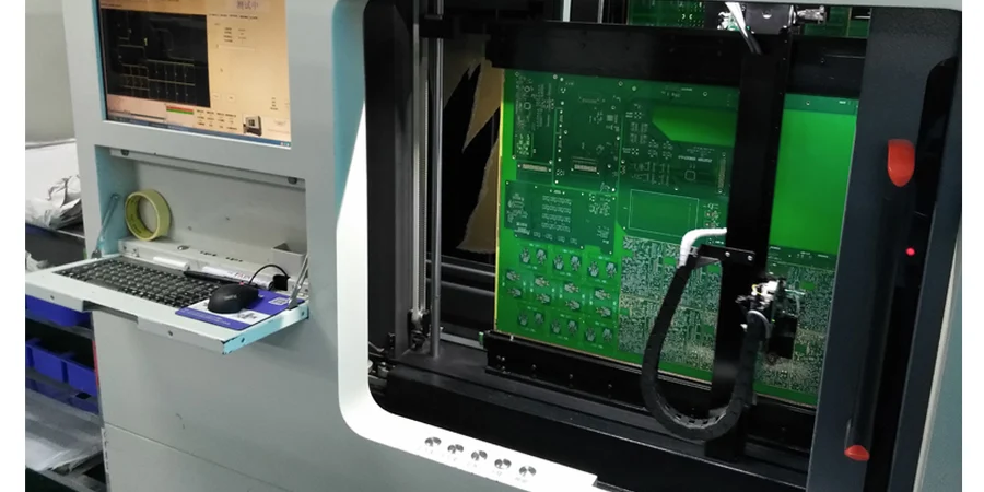
Flying probe testing is a fixtureless electrical test method in which programmable probes contact selected PCB or PCBA nodes for continuity, isolation, component, signature, or limited powered tests. On inverter electronics, its coverage must be separated from X-ray, high-voltage insulation, functional, HIL, and product-safety tests.
Key Takeaways
- Specify whether “flying probe” means unpopulated-board electrical test or assembled-board in-circuit test; they use different data, limits, and conclusions.
- Build coverage from inverter failure risks, not from a generic promise of testing every net or component.
- Flying probe can find many opens, shorts, wrong values, orientation errors, and analog-signature anomalies, but access and circuit topology limit coverage.
- It cannot see BGA voiding, prove every hidden solder joint, validate high-current capacity, or replace hipot, insulation resistance, functional, HIL, EMC, thermal, or safety tests.
- Use low-energy, unpowered checks before controlled energization, and keep high-voltage test equipment, discharge controls, and safety ownership separate.
- During NPI, fixtureless programming supports ECOs; at stable volume, compare flying probe, ICT, boundary scan, and functional fixtures by coverage, throughput, and cost.
- Release a test coverage matrix, safe-state definition, probe-access drawing, limits, golden-data method, and failure-report package with the RFQ.
Table of Contents
- Bare Board or PCBA: Which Flying Probe Test Do You Need?
- What Can Flying Probe Detect on an Inverter PCBA?
- Use a Layered Inverter Test Coverage Matrix
- Create a Safe High-Voltage Test Gate
- Design the Inverter PCB for Probe Access
- Plan Coverage for BGAs and Power Components
- Use Flying Probe Through EVT, DVT, PVT, and Production
- Turn Test Results into Process Evidence
- Test Before and After Selective Soldering and Coating
- Compare Flying Probe with ICT and Functional Test
- Diagnose Common Coverage Gaps
- Flying Probe Test RFQ Checklist
- Reference Standards and Responsibility Boundaries
- How HILPCB Supports Inverter PCB Test Planning
- Common Questions
- Conclusion
Bare Board or PCBA: Which Flying Probe Test Do You Need?
The same machine concept is used for two distinct jobs.
Bare-board flying probe electrical test compares an unpopulated PCB with an IPC-356 or other approved netlist. It checks whether intended nets are continuous and whether nets that should be separate remain isolated under the released test conditions. IPC-9252B addresses electrical testing of unpopulated printed boards and helps define test levels, data, parameters, analyzers, and fixturing.
PCBA flying probe test contacts an assembled board for in-circuit or signature measurements. Depending on equipment and access, it may check shorts, opens, passive values, diode junctions, orientation, analog signatures, or selected low-power functions. Parallel paths and inaccessible nodes can make a component impossible to isolate.
| Question | Bare PCB test | Assembled PCBA test |
|---|---|---|
| Primary input | Netlist, Gerber/ODB++/IPC-2581, drill and board geometry | CAD/netlist, BOM, pick-and-place, schematic, component models and limits |
| Main purpose | Verify fabricated connectivity and isolation | Screen assembly/component faults and support diagnosis |
| Typical defects | Opens, shorts, wrong net connectivity | Opens/shorts, missing/wrong/reversed parts, selected value/signature faults |
| Cannot prove | Assembly workmanship or product function | Hidden joint geometry, full function, high-voltage safety, power performance |
| Best timing | Before assembly | After SMT/THT steps and before expensive or irreversible operations |
An RFQ that says only “100% flying probe” is incomplete. State the board condition, source netlist, test population, limits, accessible nodes, exclusions, and required records.
What Can Flying Probe Detect on an Inverter PCBA?
Inverter control, gate-drive, sensing, communication, and auxiliary-power circuits contain many faults that can be found without applying full bus voltage. Useful checks can include:
- shorts between power, gate-drive, analog, digital, and chassis-related nets;
- opens at accessible connectors, vias, resistors, fuses, jumpers, and test nodes;
- wrong resistor or capacitor values where parallel paths allow measurement;
- reversed diodes, electrolytic capacitors, optocouplers, and other polar devices when a suitable signature is available;
- missing pull-ups, gate resistors, current-sense networks, and isolation-side support components;
- analog signatures that differ from a validated reference population;
- selected powered measurements using current-limited, isolated supplies when the procedure and equipment support them.
Coverage is not the same as accessibility. A probe may touch a node while parallel circuitry masks the component. Capacitive or vectorless techniques can detect selected IC-pin faults without direct access, but coverage remains machine-, package-, board-, and program-specific.
Ask the provider to report coverage by requirement or fault class:
| Coverage metric | Better question |
|---|---|
| Net coverage | Which opens/shorts are direct, inferred, or excluded? |
| Component coverage | Which parts have value, polarity, signature, presence-only, or no test? |
| Pin coverage | Which pins are direct, indirect, or inaccessible? |
| Safety coverage | Which checks are low-energy screens versus dedicated insulation tests? |
| Functional coverage | Which rails/interfaces are energized and protected? |
Use a Layered Inverter Test Coverage Matrix
No single test method closes all renewable-energy inverter risks. The most useful differentiating asset is a matrix that maps each failure mode to the earliest effective detection stage and the final owner.
| Risk or defect | Best early evidence | Later confirmation | Why flying probe alone is insufficient |
|---|---|---|---|
| Bare-board open or short | Netlist-based bare-board electrical test | Assembly continuity/functional test | PCBA parallel paths can hide the original conductor fault |
| Missing or wrong passive | AOI plus PCBA flying probe value/signature | Functional calibration | Measurement may be masked by parallel circuitry |
| Reversed polar part | AOI and electrical signature | Controlled power-up | Not every package or circuit yields a unique signature |
| BGA solder open | AXI, vectorless/pin technique, boundary scan where designed | Functional/interface test | Hidden joints lack direct probe access |
| BGA or power-pad voiding | X-ray/AXI and process evidence | Thermal/power validation | Electrical continuity does not measure void area or heat flow |
| HV-to-LV unintended short | Low-energy continuity/isolation screen | Dedicated IR/withstand procedure | Standard PCBA probing is not product hipot qualification |
| Creepage/clearance or contamination | Design review, AOI/visual, cleanliness evidence | Product insulation/safety tests | Electrical screen does not validate all spacing/environment conditions |
| Gate-drive timing or desaturation | Controlled functional test | Power-stage/HIL validation | Static component tests do not reproduce switching behavior |
| Current-path resistance/heating | Kelvin/DCR method where specified | Temperature-rise and load testing | Probe contact and low test current do not represent operating current |
| Control algorithm and protection | Boundary scan/programming and board functional test | HIL and system test | Flying probe does not emulate plant, grid, motor, battery, or PV behavior |
| EMC susceptibility/emissions | Layout review and pre-compliance | Accredited system EMC test | Fixtureless electrical checks do not reproduce electromagnetic stress |
Create a Safe High-Voltage Test Gate
An inverter PCBA can contain a high-voltage power domain beside low-voltage control, communication, and sensing circuits. The test strategy must prevent accidental energization, stored-energy release, and unsafe interaction between domains.
Define a safe-state document before programming:
- board population state, installed power/storage parts, and external energy sources;
- maximum stimulus, current limiting, fusing, interlocks, and operator protection;
- discharge path, wait time, verification point, and residual-voltage limit;
- prohibited probe/energization nets, isolation barriers, and guard zones;
- connection sequence and handling after a failed short or insulation screen.
Perform low-energy shorts and polarity checks before powered tests. Dedicated insulation resistance and dielectric withstand tests require equipment, fixtures, ramp/dwell limits, discharge control, and safety procedures selected from the end-product standard and insulation design. Do not reuse a bare-board isolation voltage or a flying-probe default as an inverter safety requirement.
IEC 62109-1/-2 address photovoltaic converter and inverter safety; IEC 62477-1:2022 covers power electronic converter systems within its scope. The product safety engineer determines applicability, insulation classification, sequence, and acceptance.
Design the Inverter PCB for Probe Access
Flying probe reduces dedicated fixture cost, but design for testability still improves speed, repeatability, and coverage.
Provide accessible copper for critical nets, clearance from tall components, fiducials, flat support, and a keepout map. Commercial systems differ in probe count, double-sided access, pad size, board size, height limits, and test resources. The installed machine and needle configuration set the rule.
Useful DFT decisions include:
- one accessible node on each critical rail, isolation-side reference, gate-drive channel, sensor input, and communication interface;
- test-mode controls that disable switching and place outputs in a known safe state;
- removable links, zero-ohm resistors, or isolation points that break problematic parallel paths where justified;
- Kelvin points for low-resistance shunts or current paths when DCR is an acceptance requirement;
- probe targets away from mating finishes, RF structures, wire-bond pads, and safety-critical creepage paths;
- copper and mechanical support that tolerate repeated contact without cracking or board flex;
- clear top/bottom access and component-height data;
- probe-access coordinates tied to the released board revision.
Large boards can flex under probing. Support them without contacting components, and define permitted probe marks and no-probe surfaces.
Plan Coverage for BGAs and Power Components
Flying probe cannot “verify every BGA signal and power pin” merely by touching peripheral networks. Hidden joints, common power planes, parallel pull networks, and inaccessible package nodes restrict fault isolation.
Use complementary evidence:
- AOI for visible placement and solder features;
- X-ray/AXI for hidden-joint geometry and void assessment;
- vectorless or junction techniques for selected pin faults;
- boundary scan for compatible digital interconnects;
- functional and thermal/power tests for real operation.
Void acceptance is not a universal “less than 15% IPC” rule. Criteria depend on package type, thermal pad or ball, customer drawing, applicable workmanship standard, process capability, and thermal/reliability analysis.
For IGBT, MOSFET, SiC, or GaN stages, probes may check selected gate resistors, junctions, sensing networks, and shorts. Switching loss, stability, desaturation, sharing, and thermal performance require protected functional validation.
Use Flying Probe Through EVT, DVT, PVT, and Production
Fixtureless testing is valuable when designs change frequently because program and coordinate updates are generally easier than rebuilding a bed-of-nails fixture. “Fixtureless” does not mean zero preparation: CAD normalization, library mapping, safe-state design, program generation, debug, limit setting, golden-board correlation, and fault insertion can take substantial engineering time.
| Lifecycle stage | Best use of flying probe | Release evidence |
|---|---|---|
| EVT | Screen prototypes, diagnose assembly faults, support rapid ECOs | Coverage draft, failure logs, corrected design/test data |
| DVT | Stabilize limits, correlate AOI/AXI/boundary/functional tests | Validated program, golden population, repeatability study |
| PVT | Establish yield, cycle time, escapes, retest and repair flow | Process capability and production test decision |
| Volume | 100% test, sampling audit, ECO coverage, or diagnosis as justified | Control plan, sampling rationale, maintenance and change records |
At stable volume, ICT or a functional fixture may be faster, while modern flying-probe systems can also serve production. Decide from measured cycle time and coverage, not generic minutes-versus-seconds claims.
Turn Test Results into Process Evidence
Test data supports process control only when faults are classified and traceable. More “open” calls can originate in assembly, PCB fabrication, probe contact, board support, or a program change.
Record at least:
- unit serial, board revision, lot, panel position, line and timestamp;
- program/library/limit/equipment revision;
- first-pass, retest, measured value and probe coordinates;
- confirmed cause, repair, verification and false-call classification;
- links to AOI, AXI, functional, HIL, or field data where available.
Do not publish invented PPM improvements. Establish a baseline, use confirmed root causes, and distinguish first-pass yield from final yield. Repeated retest can hide an unstable contact or marginal process.
Test Before and After Selective Soldering and Coating
Inverter assemblies often combine SMT with through-hole connectors, relays, magnetics, bus interfaces, and large capacitors. A useful gate is to test after SMT, then repeat affected coverage after selective soldering or other secondary operations. This separates defects introduced at each stage.
Before coating, complete tests that require direct copper access and repair. After coating, use visual/UV inspection, specified coverage evidence, cure records, and final functional checks. Coating can mask contamination and make rework harder if applied too early.
Define coating keepouts around connectors, test points, adjustment elements, heat-transfer interfaces, and safety features. If production probing after coating is unavoidable, specify masked targets or an approved contact/remediation process rather than puncturing the coating unpredictably.
Compare Flying Probe with ICT and Functional Test
| Method | Main strength | Main limitation | Typical role |
|---|---|---|---|
| Flying probe | Flexible, low dedicated-fixture burden, diagnostic access | Sequential motion, topology/access limits | NPI, high mix, low/medium volume, audit and diagnosis |
| Bed-of-nails ICT | Parallel contact and fast repeated in-circuit test | Fixture cost, access and ECO burden | Stable medium/high volume |
| Boundary scan | Tests supported digital interconnect without physical access to every node | Requires compatible devices and DFT | BGA/digital-chain complement |
| Functional test | Verifies powered behavior and interfaces | May diagnose poorly and miss latent structural faults | Board-level release |
| HIL | Exercises controller behavior against a simulated plant/grid | Expensive, system-specific, not a solder inspection | Algorithm, protection and system validation |
A flying-probe result can help develop ICT or functional coverage, but a golden reference must be independently verified, revision-controlled, characterized, and protected from wear.
Diagnose Common Coverage Gaps
| Gap | Why it happens | Corrective action |
|---|---|---|
| “Pass” but wrong passive remains | Parallel path masks value | Add isolation/test mode, change method, or cover functionally |
| BGA open escapes | Hidden/inaccessible pin | Add AXI, boundary scan, vectorless or functional coverage |
| False shorts on large capacitors | Charging/transient behavior | Use settling, guarding, discharge and validated limits |
| Intermittent probe calls | Oxide, coating, flex, target size, support | Improve access, cleaning, support and repeatability study |
| HV test damages low-voltage circuit | Wrong equipment/sequence or protection state | Separate low-energy screen from dedicated insulation procedure |
| Test passes before THT but fails after | Secondary soldering introduced defect | Add post-process delta coverage and traceability |
| Good board fails after program update | Library/limit/test-data change | Revision control, correlation set and approval gate |
| Coverage percentage looks high but risk remains | Metric counts easy nodes rather than critical faults | Report requirement/fault coverage and exclusions |
Flying Probe Test RFQ Checklist
Product and safety context
- Inverter type, power domains, stored energy, voltages, isolation barriers, and product standards.
- Bare PCB, SMT-only, fully assembled, coated, repaired, or another DUT state.
- Safe-state, discharge, interlock, current-limit, grounding, handling, and no-probe requirements.
Manufacturing and design data
- Manufacturing data, IPC-356 netlist, drill, BOM, centroid, schematic, drawings, and revision manifest.
- Probe-access coordinates, fiducials, support/keepout drawing, component heights, test modes, and no-contact finishes.
- Critical-net and component list: gate drive, sensing, isolation, auxiliaries, communications, protection, shunts, and power paths.
Test definition
- Separate bare-board and PCBA test requirements.
- Continuity/isolation and component/signature limits, stimulus, settling, guarding, discharge, and powered-test constraints.
- AOI/AXI, boundary-scan, IR/withstand, functional, HIL, thermal, and EOL coverage interfaces.
- Required fault coverage, explicit exclusions, golden-data method, correlation/fault-insertion plan, and repeatability target.
Production and reporting
- EVT/DVT/PVT/volume quantities, cycle-time target, sampling or 100% rationale, and retest policy.
- Equipment configuration, access, installed resources, calibration status, and program ownership.
- Raw measurements, failure coordinates, serial/lot traceability, repair loop, first-pass yield, false-call and escape reporting.
- ECO/program/library approval, data retention, material/process deviation, and revalidation triggers.
Reference Standards and Responsibility Boundaries
Use the latest contractually applicable editions and define precedence:
- IPC-9252B — Requirements for Electrical Testing of Unpopulated Printed Boards
- IPC-6012 — Qualification and Performance Specification for Rigid Printed Boards
- IPC-A-600 — Acceptability of Printed Boards
- IPC-A-610 — Acceptability of Electronic Assemblies
- J-STD-001 — Requirements for Soldered Electrical and Electronic Assemblies
- IEC 62109-1 — Safety of Power Converters for Use in Photovoltaic Power Systems, General Requirements
- IEC 62109-2 — Safety of Power Converters for Use in Photovoltaic Power Systems, Particular Requirements for Inverters
- IEC 62477-1 — Safety Requirements for Power Electronic Converter Systems and Equipment, General
- UL 1741 — Inverters, Converters, Controllers and Interconnection System Equipment for Use With Distributed Energy Resources
| Party | Responsibility |
|---|---|
| Product/safety owner | Applicable standards, hazards, insulation system, high-voltage sequence and final release |
| PCB designer | Netlist, spacing, materials, DFT access, critical nets and bare-board requirements |
| PCB fabricator | Netlist-based electrical test, workmanship, records and disclosed deviations |
| Assembly/test provider | Program, safe probing, limits, coverage, calibration, traceability and failure reports |
| Validation team | Controlled bring-up, functional, HIL, environmental, EMC, thermal and system evidence |
HILPCB can execute or coordinate the agreed manufacturing and test plan. A fixtureless continuity screen is not inverter safety approval or lifetime proof. Product safety, grid interaction, power performance, firmware, environmental, and certification decisions remain with the responsible owners and laboratories.
How HILPCB Supports Inverter PCB Test Planning
Send HILPCB the design package, safe-state document, risk matrix, probe-access drawing, test stages, limits, and report format before assembly. A useful review should return:
- separation of bare-board, assembly, insulation, functional, and system tests;
- probe-access and board-support risks;
- proposed coverage and explicit exclusions for critical nets/components;
- complementary AOI, X-ray, boundary-scan, functional, or high-voltage gates;
- program/debug, sampling, repair, reporting, cost, and schedule assumptions.
Relevant starting points include heavy copper PCB fabrication, high-thermal-conductivity PCB manufacturing, and turnkey PCBA assembly. Submit the controlled test and manufacturing package through the PCB quote request.
Common Questions
Can flying probe testing replace inverter functional or HIL testing?
No. Flying probe is primarily a structural and in-circuit screen. Functional test verifies powered board behavior, while HIL exercises the controller against a simulated grid, motor, battery, PV source, or load. Use flying probe to remove many assembly faults before those expensive stages, but retain functional, protection, calibration, and system validation.
Can flying probe testing detect BGA voids?
No. Electrical probing cannot measure internal void geometry. X-ray or AXI and a released acceptance method are needed for void assessment. Flying probe, vectorless tests, boundary scan, and functional tests can detect selected electrical faults around a BGA, but none should be described as universal hidden-joint coverage.
Is flying probe suitable for high-volume inverter production?
It can be, depending on installed machine throughput, board size, program coverage, test time, product mix, and economics. For stable high volume, compare it with fixture-based ICT and functional fixtures. Flying probe may remain useful for 100% production, sampling audits, ECOs, high-mix variants, or diagnosis.
Should flying probe be completed before conformal coating?
Complete tests that require direct copper access before coating. Also test after any process—such as selective soldering—that can introduce new defects. After coating, verify coverage/cure and run appropriate final functional checks. Use masked test targets if later probing is required; do not puncture coating without an approved process.
Conclusion
Flying probe testing adds the most value to renewable energy inverter PCBs when its role is narrow, measurable, and connected to the full validation flow. It can screen bare-board connectivity and many PCBA assembly faults without a dedicated bed-of-nails fixture, making it especially useful during design changes and high-mix production.
Release still requires layered evidence: bare-board test, AOI/AXI, PCBA probing, boundary scan, insulation, controlled power-up, functional/HIL, environmental, and product qualification. The coverage matrix prevents dangerous escapes and tests that claim too much.