
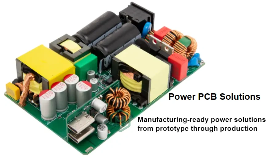
GaN power stage PCB mass production: mastering high power density and thermal challenges for power & cooling system PCB
As GaN technology matures, its adoption in power conversion is expanding rapidly—delivering unprecedented power density and efficiency. At the same time, GaN’s ultra-fast switching edges (dV/dt and dI/dt) introduce severe challenges for PCB design, manufacturing, and compliance. As an engineer focused on EMI/EMC and safety compliance, I know that successful GaN power stage PCB mass production is not just “the circuit works”—it is systematic control of safety spacing, discharge paths, filter networks, and thermal management. If these fundamentals are neglected, products can fail in certification, forcing expensive redesigns and delaying time-to-market.
From a safety + EMC compliance angle, this article covers key control points for GaN power stage PCB design and mass production—from creepage/clearance to common-mode noise suppression, grounding strategy, and manufacturing/assembly considerations. The goal is to help you build an efficient and reliable low-loss GaN power stage PCB that performs under harsh tests and real-world operating conditions.
Creepage/clearance: meeting safety requirements
In GaN high-voltage, high-frequency applications, Safety Spacing is the first line of defense against electric shock and electrical fire. It includes Clearance and Creepage.
Clearance: the shortest straight-line distance through air between conductive parts. It prevents air breakdown/arcing under overvoltage events (e.g., lightning surge). GaN systems often run on higher DC bus voltages and generate switching overshoot, so Clearance can be more demanding. Follow safety standards such as IEC 62368-1 based on working voltage, pollution degree, and material group. For example, between Primary and Secondary circuits, reinforced insulation spacing is often required.
Creepage: the shortest path along the surface of insulation. It prevents tracking under moisture/contamination. In GaN power stage PCB mass production, high power density drives very tight layouts, so Creepage is harder. Slotting (PCB cutouts) or moats are effective. Selecting higher CTI laminates (e.g., CTI ≥ 600V) increases safety margin for the same geometry.
Careful GaN power stage PCB routing is essential. Keep high-voltage traces away from low-voltage control signals and enforce a clear physical boundary between Primary and Secondary. For high-current stages, Heavy Copper PCB reduces loss and naturally increases spacing via wider conductors.
Controlling DM/CM noise: source → coupling path → victim
Nanosecond switching edges are both the source of GaN efficiency and the primary EMI generator. EMI consists of differential-mode (DM) and common-mode (CM) noise, and must be controlled systematically across source, coupling path, and sensitive circuits.
Noise source analysis:
- DM noise is driven by pulsating current in the switching loop (power loop / hot-loop), typically including the input capacitor and the half-bridge GaN devices. Minimizing loop area is the fundamental fix.
- CM noise is driven by fast-changing voltages (high dV/dt) coupling to ground (chassis/protective earth) through parasitic capacitance. Key paths include GaN Drain-to-Heatsink capacitance and transformer inter-winding capacitance.
Coupling path control:
- Minimize loop area: the core principle of GaN power stage PCB routing. Tight placement on the same or adjacent layers and vertical current paths minimize loop inductance—reducing DM noise and ringing.
- Optimize return paths: provide a clear, low-impedance return for fast switching current. In multilayer boards, a solid ground plane is ideal. For Multilayer PCB, strategic ground via stitching reduces return-path discontinuities.
Victim (sensitive circuit) protection:
- Separate noisy power areas from sensitive control/analog regions.
- Avoid routing sensitive traces across “hot” planes or near switching nodes.
- Use shielding/guarding and short reference-return paths for key signals.
Key reminder: EMC essentials for GaN PCB design
- Minimize the power loop: Place input capacitors and the GaN half-bridge as close as possible to shrink the HF current loop area—fundamental for reducing DM noise and ringing.
- Optimize gate drive: The gate-drive loop must also be minimized and use a dedicated return path; avoid mixing with power ground to preserve drive integrity.
- Strategic grounding: Clearly separate PGND, SGND, and chassis ground. Use star or local single-point connections to keep noisy PGND currents from polluting control circuitry.
- Parasitics control: GaN is extremely sensitive to parasitic inductance and capacitance; precise routing and placement are critical for stability.
Discharge paths and Y-capacitors: balancing safety and EMC
In isolated power supplies, the Y-capacitor (Y-capacitor) across Primary and Secondary (or PE) is a key filter component that provides a low-impedance return for CM noise and can significantly improve EMI. But it must balance EMC benefit against safety risk.
EMC role of Y-capacitors: Y-caps shunt CM current measured at earth (via LISN), which is key for passing Conducted Emissions (CE). Placement should be as close to the noise source as possible, typically between the grounds of the transformer’s primary and secondary sides.
Safety—leakage current: Y-caps create an AC path between Primary and Secondary (or earth), producing leakage current. Standards such as IEC 62368-1 impose strict limits (often hundreds of microamps depending on application). Therefore, capacitance cannot increase indefinitely; use safety-rated Y1/Y2 capacitors.
Bleeder resistor: for X-capacitors across line/neutral, stored charge after power-off can cause shock. Safety standards require a bleeder resistor to discharge to a safe voltage within a defined time (e.g., 1 second).
In design, you must calculate total Y-capacitance to control leakage current, and use layout tactics (e.g., series multiple small capacitors) to achieve filtering. This discipline applies from GaN power stage PCB low volume validation through mass production.
Ground strategy: partitioning and connecting chassis/signal/power grounds
Correct grounding is the foundation of stable, reliable, compliant GaN power systems. Messy grounding is one of the largest causes of EMI.
- PGND: carries high-current switching loops and is full of HF noise. Keep it short and wide to lower impedance.
- SGND/AGND: reference for controllers, sensing, and sensitive analog/digital signals. Keep it “clean” and isolated from PGND noise.
- Chassis Ground / PE: tied to the enclosure and earth; final barrier for EMI shielding and safety.
Partition and connection tactics:
- Physical separation: partition PGND and SGND areas on the PCB. Typically SGND connects to PGND at only one point (under the controller or at the power input), forming star/single-point grounding to prevent PGND noise currents from flowing through SGND.
- Kelvin connection: for current shunts and precision measurement parts, use 4-wire Kelvin routing to separate current paths from sense paths and avoid lead resistance/noise coupling.
- Chassis connection: Y-cap ground, input filter ground, and EMI shielding cans commonly connect to chassis ground. The location/method strongly affects Radiated Emissions (RE).
For high thermal demand GaN systems, the heatsink itself can become a noise antenna. If it must be grounded, choose between PGND and chassis ground based on test data—validated via GaN power stage PCB testing. Materials like High Thermal PCB can improve thermal behavior but may introduce new parasitic capacitance paths that must be included in grounding strategy.
GaN vs. Si MOSFET: PCB design rule comparison
| Design parameter | Traditional Si MOSFET PCB | GaN power stage PCB |
|---|---|---|
| Switching frequency | Tens to hundreds of kHz | Hundreds of kHz to several MHz |
| Power-loop inductance | More tolerant (nH range) | Extremely strict (sub-nH) |
| Gate-drive requirement | Standard drive; moderate layout sensitivity | High-speed, low-impedance drive; extremely layout-sensitive |
| Thermal management | Primarily heatsink + standard packages | Board-level thermal (thermal vias, embedded copper) |
| Safety spacing | Standard requirements; easier to meet | Very challenging due to dense layout |
Input filter selection: CM choke, DM inductor, and capacitor network
The input EMI filter is the final gatekeeper for passing Conducted Emissions. A good filter suppresses noise below limits without hurting efficiency or stability.
CM choke: the core element for CM noise suppression. Key selection points:
- Impedance spectrum: the impedance peak should cover the main GaN noise spectrum (often 1–30MHz).
- Rated current: must handle max current without saturation.
- Parasitic capacitance: inter-winding capacitance creates a high-frequency bypass that degrades choke performance; select low-parasitic designs.
DM inductor / X-capacitor: form an LC or Pi filter to attenuate DM noise.
- X-cap: placed at the input to provide a low-impedance path for DM noise; low ESL/ESR matters.
- DM inductor: consider inductance retention at high frequency and DCR (directly impacts efficiency)—a key factor for a low-loss GaN power stage PCB.
Filter layout matters as much as component selection. Treat the filter as an independent physical block at the power entry and define a clear “dirty” side (input) and “clean” side (output) to prevent re-coupling of external noise into filtered nets.
From prototype to production: manufacturing and assembly considerations
A lab-perfect GaN power stage PCB quick turn prototype can run into surprises in mass production. Successful GaN power stage PCB mass production depends on building DFM (Design for Manufacturability) and DFA (Design for Assembly) thinking into the design early.
- Terminals/connectors: high-current input/output terminals must carry current and be mechanically robust. Pin Creepage/Clearance must also satisfy safety requirements.
- Shielding can: if radiated emissions are over limits, adding a metal shielding can over the switching stage can help. It must connect well to PCB ground at multiple points.
- Ground springs/screw holes: when tying PCB ground to the metal enclosure, use grounding springs or large ground copper around screw holes with solder mask removed to ensure a low-impedance connection.
Partnering with a reliable manufacturer matters. For example, HILPCB’s Turnkey Assembly provides end-to-end quality control from component sourcing to fabrication and final assembly.
Assembly strengths: ensuring consistent GaN PCB performance
- Precision placement: GaN packages are small and sensitive to thermal stress. Advanced SMT equipment and controlled reflow profiles protect devices from damage.
- Thermal interface handling: For bottom-cooled GaN devices, uniform solder paste and low voiding are critical for heat transfer. X-Ray verifies solder quality.
- Consistency control: From **GaN power stage PCB low volume** pilot runs to high volume, strict SPC keeps parasitics and performance consistent board-to-board.
- Functional & safety testing: Provide FCT and hi-pot insulation tests so every shipped unit meets design specs and safety requirements.
Comprehensive validation: why GaN power stage PCB testing matters
Design and manufacturing results must be validated by rigorous testing. Comprehensive GaN power stage PCB testing is the “passport” to compliant product launch.
- Conducted Emissions (CE): use LISN to measure line-conducted noise from 150kHz to 30MHz—key for evaluating input EMI filter performance.
- Radiated Emissions (RE): in an anechoic chamber, measure radiated fields from 30MHz to 1GHz (or higher). Layout, grounding, and shielding drive results.
- Immunity tests:
- ESD: simulate electrostatic discharge to evaluate protection.
- EFT: simulate fast transient bursts on power lines to evaluate filtering on power and I/O.
- Surge: simulate lightning or grid switching surges to evaluate primary protection (MOV, TVS).
Test results are valuable inputs for iteration. A failed test is not “the end”—it is an opportunity to pinpoint issues. By analyzing failing frequencies and modes, engineers can tune GaN power stage PCB routing, filter parameters, or grounding strategy.
Conclusion
GaN power stage PCB mass production is a cross-disciplinary system engineering challenge. It requires not only power electronics expertise but also deep EMI/EMC and safety compliance know-how. From macro safety spacing and ground partitioning to micro loop control and parasitics management, every detail can decide success.
By applying the strategies discussed—strict safety spacing, systematic source-path-victim noise control, balancing Y-capacitor EMC vs safety, structured grounding, careful filter design, and manufacturability-aware implementation—you can significantly raise first-pass certification success. Working with an experienced manufacturing partner like HILPCB helps translate complex design intent into high-quality, reliable products—whether GaN power stage PCB quick turn prototypes or high-volume builds—so your design advantage becomes a market advantage.
Common Questions
Why is GaN power stage PCB mass production especially challenging?
Because GaN designs combine fast switching edges, EMC sensitivity, safety spacing requirements, and manufacturability constraints in the same product. Small design or process mistakes can quickly turn into certification failures or unstable field performance.
Why do safety spacing and EMI control have to be considered together on GaN boards?
If they are handled separately, one fix can easily create a new problem elsewhere. The layout has to balance creepage, clearance, grounding, filtering, and parasitic control as one coordinated system.
Why is manufacturability important for GaN certification success?
A design that works in theory can still fail if production variation changes parasitics, spacing, or assembly quality. Building manufacturability into the layout and process helps maintain the consistency needed for first-pass testing and later mass production.
Why should teams work with an experienced manufacturing partner on GaN power products?
GaN power stages sit at the intersection of power electronics, EMC, safety, and production engineering. A capable partner can translate the design intent into repeatable fabrication, assembly, and validation practices instead of leaving critical risks to trial and error.