
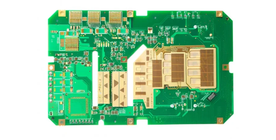
At the peak of the AI and HPC wave, every leap in compute depends on breakthrough hardware beneath. HBM3 (High Bandwidth Memory) and its evolution are now key to breaking the memory wall and enabling full AI-chip performance. But the bridge that connects GPU/TPU cores to HBM3 memory stacks—the Interposer and the organic substrate PCB carrying it—faces unprecedented reliability pressure. As an engineer responsible for mass-production validation, I know HBM3 interposer PCB reliability is not just a metric; it determines whether AI accelerators worth tens of thousands of dollars can run stably for years in harsh data-center environments.
These advanced 2.5D/3D packaging modules often exceed 1000W, with data throughput reaching TB/s. Under such extreme conditions, any tiny design flaw, material defect, or process deviation can be amplified into system failure. Systematically solving HBM3 interposer PCB reliability is therefore the foundation of end-to-end success—from design and fabrication through mass-production validation. Leading manufacturers such as Highleap PCB Factory (HILPCB) help customers address these complex interconnect challenges through advanced process capability and strict quality control.
What fundamentally drives HBM3 Interposer PCB reliability challenges?
To understand HBM3 interposer PCB reliability, you must recognize its unique position in the AI-package ecosystem. It is no longer a “traditional PCB” in the usual sense; it is the convergence point between semiconductor packaging and system-level interconnect—often part of 2.5D structures like CoWoS (Chip-on-Wafer-on-Substrate). In this architecture, the logic die (GPU) and HBM stacks are placed side-by-side on a Silicon Interposer, and the whole module is then packaged onto a high-performance organic substrate.
This architecture creates three core sources of reliability challenge:
Thermomechanical Stress: High TDP creates extreme heat flux. Different materials in the package (silicon, copper, organic substrate, solder) have very different CTE. Under repeated power cycling (power on/off or workload transitions), CTE mismatch generates large mechanical stress at interfaces and microstructures—driving physical failures such as cracks and delamination.
Electrical Performance Demands: HBM3 has thousands of I/O channels, each running at 6.4 Gbps+. Signals travel on micron-scale structures and are extremely sensitive to impedance variation, crosstalk, and power noise. Any small electrical degradation can raise BER and reduce stability—an electrical-reliability problem.
Manufacturing Process Limits: To achieve dense interconnect, line/space can be ~10µm or below and stacked Microvias are heavily used. These structures demand extreme precision and consistency. Process deviations—uneven plating, misregistration, lamination defects—become latent reliability risks.
How thermomechanical stress gradually erodes interposer integrity
From a mass-production validation perspective, Thermal Cycling is a core method for long-term reliability assessment. We repeatedly emulate temperature transitions from cold start to full load (e.g., JEDEC -40°C to 125°C) to accelerate exposure of thermomechanical weaknesses.
Common failure modes include:
- Microvia cracking: Microvias connect layers. Under thermal stress, CTE mismatch between copper plating and dielectric concentrates stress at corners/bottoms. Over long cycling, fatigue cracks form and ultimately create opens—especially critical for stacked microvia structures.
- Pad Cratering: Under BGA balls, stress can concentrate at the pad/substrate interface. Board deformation from heat or mechanical shock can crack resin beneath pads, creating a hard-to-detect hidden failure.
- Delamination: At interfaces between copper, dielectric (e.g., ABF), and core, insufficient adhesion plus moisture ingress can cause interface separation under expansion/contraction, severely impacting SI and thermal performance.
To mitigate these issues, selecting high Tg and low Z-axis CTE High Tg PCB materials is critical. These laminates maintain better dimensional stability and mechanical strength at high temperature—improving thermomechanical reliability significantly.
Key thermomechanical failure modes and mitigation strategies
| Failure mode | Root cause | Design/manufacturing mitigations |
|---|---|---|
| Microvia cracking | Copper fatigue driven by CTE mismatch | Optimize microvia structure (copper filling), control plating ductility, select low-CTE materials |
| Pad cratering | Stress concentration under pads | Use NSMD design, improve resin toughness in base materials |
| Delamination | Insufficient interlayer adhesion, moisture ingress | High-adhesion materials, strict lamination control, thorough bake before shipment |
Why HBM3 Interposer PCB impedance control cannot slip
At HBM3 data rates, transmission-line effects are extreme. Every segment must be treated as a precision transmission-line system whose characteristic impedance matches driver and receiver. The importance of HBM3 interposer PCB impedance control cannot be overstated.
Impedance mismatch causes reflections—like light reflecting off a mirror. Reflections superimpose on the signal, creating distortion, ringing, and eye closure that leads to data misinterpretation. With a 1024-bit-wide HBM3 interface, even intermittent errors on a single channel can crash the whole system.
Achieving accurate impedance control requires design and manufacturing to work together:
- Design phase: Engineers use professional field solvers to compute trace geometry based on Dk/Df, trace width, dielectric thickness, and spacing to reference planes.
- Manufacturing phase: The manufacturer must control etched width, laminated dielectric thickness, and material Dk/Df consistency to match the design. Tolerances typically need to be within ±5%, which is a major challenge at IC substrate PCB level.
Experienced manufacturers like HILPCB use TDR and related equipment to sample or fully inspect impedance per lot, ensuring delivered products meet strict electrical requirements.
What are the core principles of robust HBM3 Interposer PCB design?
Reliable HBM3 interposer PCBs start with robust design. This is a system engineering problem, not just “connecting nets”. Below is a concise HBM3 interposer PCB guide of core principles:
Symmetric and balanced stackup: Stackups must be strictly symmetric. Asymmetry causes different layer shrink rates during thermal processes (e.g., reflow), driving severe Warpage. Warpage can be catastrophic for downstream die attach and assembly.
Well-planned PDN: AI chips have extreme transient current demand. PDN design targets stable, clean power under all workloads via low-impedance power planes, sufficient decoupling close to pins, and tight loop-inductance control to minimize IR Drop and power noise.
No-compromise SI strategy:
- Reference-plane continuity: Every high-speed net must have a continuous reference plane (GND or VCC) underneath—foundational for HBM3 interposer PCB impedance control.
- Crosstalk control: Maintain spacing between parallel traces (commonly the 3W rule: spacing > 3x trace width) to reduce EM coupling.
- Via optimization: Vias are discontinuities. Minimize via count and optimize structures (e.g., backdrill to remove stub) to reduce reflections.
Great HBM3 interposer PCB design is the best balance across performance, cost, and manufacturability. Early collaboration with an experienced DFM supplier like HILPCB helps avoid expensive redesigns and schedule slips later.
Interposer substrate material comparison
| Metric | Standard FR-4 | High Tg FR-4 | ABF-like build-up materials | Reliability impact |
|---|---|---|---|---|
| Tg | ~140°C | >170°C | >200°C | Higher Tg improves high-temp dimensional stability and delamination resistance. |
| CTE (Z-axis, ppm/°C) | 50-70 | 40-60 | <40 | Lower CTE reduces mismatch to silicon/copper and lowers thermomechanical stress. |
| Dk (@10GHz) | ~4.5 | ~4.2 | <3.5 | Lower Dk improves propagation speed and reduces crosstalk. |
| Df (@10GHz) | ~0.020 | ~0.015 | <0.005 | Lower Df reduces attenuation and is critical for [High Speed PCB](/products/high-speed-pcb). |
How HBM3 Interposer PCB routing strategies impact reliability
High density is one of the defining characteristics of HBM3 interposer PCBs. In a tiny footprint, you must route thousands of high-speed signals along with power and ground. HBM3 interposer PCB routing is extremely challenging and directly impacts electrical reliability and manufacturability.
Key routing considerations:
- Escape Routing: Breaking out signals from µBGA pads is the first challenge. This typically requires multi-layer HDI structures, using microvias directly from pads into inner layers. Routing channel planning must be done early.
- Length Matching: For parallel buses like HBM3, DQS/DQ lengths must be tightly matched to keep timing aligned. “Serpentine” tuning is often required, increasing routing complexity.
- Avoid sharp corners and stubs: Avoid 90° corners; use 45° or arcs to reduce impedance steps and reflections. Avoid stubs on high-speed nets because they become reflection sources.
Complex HBM3 interposer PCB routing requires advanced EDA tools and experienced engineers. Poor routing sacrifices electrical performance and can also drive manufacturing issues such as Acid Traps, hurting etch quality and creating latent reliability risk.
What qualifies as an industrial-grade HBM3 Interposer PCB?
An industrial-grade HBM3 interposer PCB means it not only performs in lab conditions, but also survives years of 7x24 operation in real data-center deployments. This demands top-tier standards across materials, manufacturing, and testing.
- Core materials: Typically Ajinomoto Build-up Film (ABF) or equivalent advanced build-up dielectrics. These offer low Dk/Df, high thermal resistance, low CTE, and strong laser-drilling performance—forming the basis for high density and high reliability.
- Manufacturing precision:
- Line capability: line/space reaching 15/15µm or finer.
- Registration: layer-to-layer registration must be tightly controlled to ensure reliable microvia connections.
- Plating uniformity: surface finish and copper filling must be highly uniform to ensure impedance consistency and current capacity.
- Strict reliability validation: Beyond standard thermal cycling, industrial-grade HBM3 interposer PCB must pass harsher tests, such as:
- HAST: evaluates moisture resistance under high temperature, high humidity, and pressure.
- TCT: evaluates via reliability under repeated thermal shock.
- Mechanical shock and vibration: simulates mechanical stress during shipping and operation.
Only with this full qualification flow can you ensure stable reliability across the full lifecycle.
HILPCB IC substrate-level manufacturing capabilities
| Parameter | HILPCB capability | Parameter | HILPCB capability |
|---|---|---|---|
| Max layers | 32 Layers | Min line/space | 1.0/1.0 mil (25/25 µm) |
| Board thickness | 0.2 - 3.2 mm | Min mechanical drill | 0.1 mm |
| Min laser microvia | 50 µm | Impedance tolerance | ±5% |
| Supported materials | ABF, BT, High Tg FR-4 | Surface finish | ENEPIG, Immersion Tin/Silver |
Which manufacturing processes and defect controls are mandatory?
From a validation engineer’s view, manufacturing defects are direct sources of reliability issues. For HBM3 interposer PCBs, key process controls include:
- Build-up Process: The core process for HDI and IC substrates. Each dielectric layer (e.g., ABF film) and copper foil is laminated layer-by-layer. Temperature, pressure, and vacuum control must be extremely precise to prevent delamination and voids.
- Laser Drilling: Microvias are formed by high-precision laser ablation. Laser energy, spot size, and focus location affect via geometry and quality. Poor drilling makes plating difficult and creates weak interconnect points.
- Copper Filling: Microvias often require fully filled copper to ensure electrical and thermal performance. This needs specialized chemistry and current control to achieve void-free filling. Any void becomes a stress concentrator and a potential open-failure point.
- AOI/AXI: With ultra-fine routing, manual inspection is insufficient. AOI detects surface opens/shorts/etch defects. For complex buried microvia structures, AXI is often the only effective way to verify internal connectivity integrity.
In volume production, we monitor SPC data on these key processes and perform DPA (e.g., microsection analysis) to ensure manufacturing stays under control.
How does HILPCB protect end-to-end reliability for your AI program?
With challenges this complex, choosing a technically strong and experienced manufacturing partner is critical. HILPCB provides an end-to-end solution to systematically ensure HBM3 interposer PCB reliability:
Our methodology is built on four pillars:
- Forward-looking design collaboration: Engage early with our engineering team. With DFM/DFA analysis, we help optimize HBM3 interposer PCB design, avoid manufacturing traps, and improve reliability at the source.
- Top-tier materials and processes: HILPCB continuously invests in advanced manufacturing and materials science, with deep expertise across high-performance substrates including ABF. Strict process control ensures strong electrical performance and thermomechanical stability on every shipped PCB.
- End-to-end quality monitoring: A full QA system from IQC to IPQC to FQC, combined with AOI, AXI, TDR impedance testing, and comprehensive reliability testing, ensures 100% conformance to spec.
- Turnkey manufacturing and assembly: Beyond PCB fabrication, HILPCB provides integrated SMT Assembly and Turnkey Assembly. This vertical integration avoids cross-vendor coordination gaps and ensures process compatibility from bare-board to chip mounting—delivering unified reliability assurance.
Conclusion
HBM3 interposer PCB reliability is not a single isolated challenge, but the ultimate test of end-to-end capability across design, materials, manufacturing, and validation. It is a system engineering outcome jointly determined by thermomechanical stability, electrical integrity, and manufacturing excellence. As AI chips push toward higher compute and better efficiency, reliability requirements for the underlying interconnect will only intensify.
For organizations building next-generation AI hardware, ignoring interposer PCB reliability is like building a skyscraper on an unstable foundation. By understanding failure mechanisms, adopting robust design principles, and partnering with a manufacturer like HILPCB with deep expertise and strict quality control, you can manage these complex challenges and keep your innovations competitive. Contact us to start your high-reliability AI interconnect program.