
The HDI circuit board is the backbone of modern electronics—delivering compact size, faster speed, and higher reliability in today’s connected world. As devices evolve toward 5G, IoT, and AI-driven applications, HDI technology enables designers to pack more performance into smaller, lighter, and more efficient products.
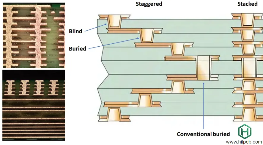
Through advanced microvia, blind, and buried via structures, HDI circuit boards improve signal integrity, reduce power loss, and support higher data rates for critical systems like smartphones, automotive electronics, and medical devices. This makes HDI an essential platform for achieving both miniaturization and high functionality.
At HILPCB, we specialize in manufacturing precision-engineered HDI circuit boards for high-speed, high-density applications. Combining advanced materials, controlled impedance design, and automated HDI PCB manufacturing & assembly, we help global OEMs accelerate innovation and bring smarter electronics to market faster.
1. Why HDI Circuit Boards Matter in Next-Generation Design
Traditional multilayer PCBs can no longer support today’s miniaturized electronics. Devices like 5G smartphones, smartwatches, and AR headsets require ultra-dense interconnections to fit high-speed processors, memory, and sensors within limited space.
HDI circuit boards achieve this through:
- Microvias as small as 0.075 mm for dense inter-layer connections
- Reduced layer count with improved electrical performance
- Lower parasitic capacitance and inductance for cleaner high-speed signals
- Enhanced reliability through shorter current paths and reduced heat buildup
These advantages make HDI the backbone of devices requiring both signal precision and compact size—from 5G mobile SoCs to wearable biosensors.
2. Applications of HDI Circuit Boards
1. 5G Mobile and RF Systems
With frequencies above 28GHz, 5G modules require ultra-low-loss substrates and microvia interconnects for antenna arrays, baseband processors, and RF front ends. HDI designs ensure minimal signal delay and reflection.
2. IoT and Smart Devices
In IoT modules and edge sensors, HDI allows system-in-package (SiP) integration and lower power consumption—ideal for battery-operated environments.
3. Electric Vehicles (EVs) and ADAS
High-density PCBs in control and infotainment units improve signal routing efficiency and thermal balance, reducing failure risk in automotive-grade environments.
4. Medical Wearables and AR/VR Devices
Flexible HDI circuit boards support rigid-flex hybrid designs for compact, comfortable, and high-performance wearables.
3. Engineering Challenges in HDI Circuit Board Manufacturing
Miniaturization introduces manufacturing complexity. To ensure precision and reliability, we employ advanced fabrication processes across every step:
- Laser Drilling for Microvias — ensuring via diameter uniformity within ±10 μm.
- Sequential Lamination — building stacked vias for multi-depth interconnects up to 20+ layers.
- Copper Filling and Via-in-Pad — improving current flow and reducing inductance in BGA packages.
- Controlled Impedance Testing — ensuring signal integrity for high-speed lines such as PCIe Gen5/6 and LPDDR5.
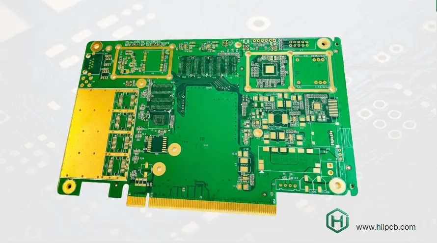
Every HDI circuit board is validated with X-ray inspection, cross-section analysis, and electrical testing to meet IPC Class 3 reliability standards.
4. Materials and Design Optimization
Material choice plays a decisive role in HDI board performance.
We offer multiple substrate options based on target applications:
| Application | Recommended Material | Key Advantage |
|---|---|---|
| 5G RF Modules | Low-loss hydrocarbon ceramic | Excellent dielectric stability |
| Automotive Electronics | High-Tg FR-4 | Superior heat and vibration resistance |
| Consumer Wearables | Polyimide & Flexible Core | Lightweight and bendable |
| AI Edge Devices | Hybrid FR-4 + Megtron 6 | Low Df for high-speed signal lines |
Our engineers perform DFM (Design for Manufacturability) and DFT (Design for Test) reviews early in the design stage, optimizing stack-up and signal paths to minimize production risks.
5. Advantages of Partnering with HILPCB
Choosing HILPCB for your HDI circuit board manufacturing means gaining access to a vertically integrated production ecosystem:
- Turnkey Manufacturing — from design validation to SMT assembly and testing under one roof.
- High-Speed Capability — compatible with high-speed PCB and rigid-flex PCB solutions.
- Scalable Volume Options — from small batch assembly prototypes to large volume assembly.
- Stringent QA — including TDR testing, reliability analysis, and IPC-6012 Class 3 certification.
Our global logistics and engineering teams ensure rapid response and quality consistency—whether you’re developing a wearable PCB or mass-producing a 5G router module.
6. Future Trends: HDI Circuit Boards in AI Edge and 6G Systems
As AI computation moves closer to the edge and 6G technology emerges, HDI circuit boards will play an even greater role in achieving compact yet powerful architectures.
Future developments include:
- Hybrid HDI–substrate integration for advanced packaging
- Embedded passives for shorter signal paths
- Ultra-low Df materials for 224G data rates
- Enhanced heat dissipation for AI accelerators
These innovations ensure that HDI remains the core interconnect technology powering the next wave of intelligent, connected devices.
FAQ
Why is an HDI circuit board different from a traditional multilayer PCB?
An HDI circuit board is built to increase routing density and electrical performance within a tighter area, not just to add more layers. It relies on finer lines, smaller vias, laser-drilled microvias, and more precise stack planning so advanced packages and compact systems can be routed without sacrificing signal quality or manufacturability.
When do designers really need HDI instead of a conventional PCB approach?
HDI becomes necessary when component pitch, escape routing, form-factor pressure, or high-speed interconnect demands exceed what a standard through-hole via structure can handle efficiently. If a design can no longer meet size, layer count, or signal objectives without excessive compromises, HDI is usually the practical next step.
What makes HDI manufacturing more difficult than standard PCB fabrication?
The challenge comes from tight registration windows, microvia quality, sequential lamination control, and the sensitivity of fine features to process variation. A small drift in drilling, plating, or lamination can impact reliability and yield, so HDI success depends on disciplined process capability rather than only on nominal design intent.
What should teams validate before moving an HDI board into scale production?
They should validate escape routing robustness, via reliability, stack-up repeatability, assembly compatibility, and the board's electrical performance under real operating conditions. It is also important to confirm that prototype results can be reproduced consistently in volume, especially when the design depends on stacked microvias, fine-pitch BGAs, or high-speed channels.
Conclusion
The rise of connected intelligence—spanning AI, edge computing, and 6G communication—depends on the ability to transmit data faster and more efficiently within compact architectures. The HDI circuit board stands at the center of this transformation, enabling the dense routing and signal precision required by next-generation electronic systems. As form factors shrink and performance expectations climb, HDI technology bridges the gap between design ambition and manufacturable reality.
At HILPCB, we view each HDI circuit board as more than a substrate—it’s the foundation of product innovation. Our end-to-end capabilities—from design verification and material selection to HDI PCB assembly and mass production—ensure electrical performance, mechanical reliability, and scalability. Every project is supported by in-house testing, simulation, and global logistics to help clients accelerate development cycles and reduce risk.
In conclusion, HDI circuit boards are no longer optional—they are essential for companies striving to compete in high-frequency, high-density, and high-reliability markets. By partnering with HILPCB, OEMs and technology leaders can transform complex designs into durable, high-performance products built for the connected future. Together, we build the circuits that power the next wave of intelligent devices.