
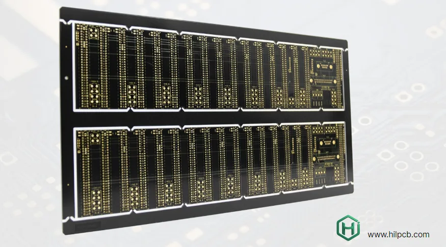
An HDI PCB is a high-density interconnect printed circuit board that uses fine conductors, small capture pads, blind or buried vias, and usually laser-formed microvias to route more connections in less area than a conventional through-hole multilayer board. HDI is useful when package escape, board size, or interconnect density demands it—not simply because a product is high-speed or advanced.
Key Takeaways
- Use HDI when a fine-pitch BGA, via-in-pad requirement, routing bottleneck, or size limit cannot be solved cleanly with a standard multilayer stack-up.
- A 1+N+1 stack-up has one sequential build-up layer on each side of a central core; 2+N+2 adds another build-up cycle and routing layer per side.
- Staggered microvias usually consume more area but avoid the stacked interface. Stacked structures save space but demand controlled copper fill, registration, and reliability evidence.
- Microvia diameter, dielectric depth, aspect ratio, capture pad, fill method, and stacked-via count must be approved as one fabricator-specific structure.
- The main HDI cost drivers are sequential lamination cycles, laser-drill programs, via filling and planarization, fine line/space, material, inspection, and yield—not the label “HDI.”
On this page
- What makes an HDI PCB different?
- When should you use HDI instead of a standard multilayer PCB?
- Which HDI stack-up should you choose?
- How should microvias and via-in-pad be designed?
- How do stack-up and materials affect signal integrity?
- How is an HDI PCB manufactured?
- What causes HDI microvia failures?
- What drives HDI PCB cost?
- What should be included in an HDI PCB RFQ?
- Reference standards and scope
- Why manufacture HDI PCBs with HILPCB?
- FAQ
What makes an HDI PCB different?
Conventional multilayers rely mainly on plated through-holes that consume space on every crossed layer. HDI adds blind microvias, buried vias, and via-in-pad transitions under component lands.
Short microvias reduce stubs and free BGA routing channels, but excessive stacking, small capture margins, or unbuildable dielectric depth can reduce yield and reliability.
| Feature | Conventional multilayer | HDI PCB |
|---|---|---|
| Main vertical interconnect | Plated through-hole | Microvia plus blind, buried, or through vias |
| Fine-pitch escape | Dog-bone fanout where space permits | Via-in-pad and microvia fanout |
| Lamination | Often one main lamination | One or more sequential build-up cycles |
| Routing impact | Through-holes block channels on crossed layers | Blind connections preserve unrelated inner-layer routing |
| Main process risk | Drill registration and through-hole plating | Laser formation, fill, planarization, registration, and microvia interfaces |
When should you use HDI instead of a standard multilayer PCB?
Choose the simplest construction that routes the board. More conventional layers may be cheaper than microvias, but cannot help when through-hole pads still block dense-package escape.
| Design condition | Start with standard multilayer | Consider HDI |
|---|---|---|
| Component escape | Coarser BGA can use dog-bone fanout | Fine-pitch or high-I/O BGA needs via-in-pad |
| Board area | Outline has routing room | Fixed outline or thickness prevents expansion |
| Via stubs | Electrically acceptable or backdrillable | Blind transitions materially simplify critical channels |
| Routing density | Through-via keepouts still leave channels | Via fields block required inner-layer routing |
| Cost priority | Lowest process complexity | Smaller area or fewer total layers may offset build-up cost |
A high-speed PCB may use ordinary through-holes, while a low-speed wearable can require HDI solely for package density.
Which HDI stack-up should you choose?
IPC-2226A defines six types: Type I uses one HDI layer on one or both core sides; Type II adds buried core vias; Type III uses two or more HDI layers; Types IV–VI cover passive-core, coreless, and alternate constructions.
In i+N+i, “i” is the build-up count per side and “N” is the core, directly describing the manufacturing sequence.
| Structure | Use it when | Avoid it when | Main verification need |
|---|---|---|---|
| Standard multilayer | Through-via escape and layer count are acceptable | Package density blocks routing | Drill-to-copper and any high-speed stub analysis |
| 1+N+1 | One adjacent-layer microvia step releases the BGA or surface routing | Nets require repeated deep transitions | Laser depth/diameter, registration, fill and planarization |
| 2+N+2 | Two build-up layers are needed for fanout or routing | A simpler stack can route the board | Each sequential lamination and microvia interface |
| Stacked microvias | Maximum density requires aligned transitions | Reliability target or fab data does not support the stack | Copper fill, interface quality and thermal-stress validation |
| Staggered microvias | Routing has room to offset transitions | Escape area is too restricted | Land geometry, local routing and copper balance |
| Any-layer/ELIC | Multiple dense packages require layer-to-layer freedom | Volume, cost, and qualification do not justify it | Full process capability and product-specific reliability plan |
The practical rule is to stop at the first structure that routes. A speculative 3+N+3 or any-layer stack adds lamination, registration, fill, and yield risk without improving the product if 1+N+1 already works.
How should microvias and via-in-pad be designed?
A microvia is not a scaled-down through-hole. Diameter and depth depend on laser process, dielectric, copper, target-pad access, and plating. HILPCB lists 0.10 mm standard and 0.05 mm advanced laser holes with typical 0.8:1 to 1:1 aspect ratios; final values require stack-up review.
Via-in-pad under a BGA normally requires filling and planarization. An open or poor cap can drain solder or distort the pad. Specify fill, cap, planarization, and plating instead of leaving “VIPPO” unexplained.
Provide a via table with layer span, diameter, pads, fill/cap, stack or stagger relationship, and via-in-pad status. Avoid multiple microvia geometries per build-up layer without approval.

How do stack-up and materials affect signal integrity?
The stack-up still controls impedance, loss, returns, crosstalk, and power distribution. Place reference planes beside critical signals and return transitions near layer changes; a short microvia cannot repair a broken return path.
Choose stocked dielectric constructions that meet impedance and laser needs. Thin dielectrics help aspect ratio and plane coupling but increase manufacturing sensitivity. Match Dk, Df, copper roughness, glass/resin system, Tg, z-axis expansion, and reflow exposure to the real budget.
Microvias can assist local heat spreading but cannot replace adequate planes, via arrays, thermal pads, or mechanical heat transfer. Validate the real copper structure thermally.
How is an HDI PCB manufactured?
A 1+N+1 flow builds the core, forms buried vias, laminates outer dielectric/copper, laser-drills and plates microvias, images circuitry, then completes mask, finish, profile, and electrical test.
Each added build-up repeats lamination, laser drilling, plating, filling, and imaging. Registration error and material movement accumulate, making copper balance, scaling, target recognition, and alignment essential.
Use AOI, X-ray alignment checks, cross-sections, electrical test, and specified TDR coupons. Agree evidence before fabrication because electrical test alone may miss a latent interface weakness.
What causes HDI microvia failures?
Lamination, reflow, test, and field cycling can expose weak plating, target-pad bonding, voids, contamination, or stacked-interface stress.
| Risk or symptom | Likely contributor | Prevention or evidence |
|---|---|---|
| Open after reflow or cycling | Weak microvia-to-target interface, void, inadequate copper | Process coupons, cross-section, resistance monitoring and representative thermal exposure |
| Failure in a stacked column | Multiple aligned interfaces and accumulated z-axis stress | Reduce stack count, use staggered vias where routing permits, qualify the exact stack |
| Pad depression or poor BGA joint | Incomplete fill or planarization | Fill/cap specification, surface-planarity inspection and assembly review |
| Registration breakout | Material movement or insufficient capture margin | Fabricator scaling, X-ray registration checks and approved land geometry |
| Cracking near resin/copper boundary | Material CTE mismatch or severe thermal history | Material review, controlled lamination/reflow and product-specific cycling |
| High resistance or intermittent net | Plating defect, contamination, damaged interface | Four-wire coupon monitoring where required and continuity after stress |
Define construction, acceptance class, thermal history, environment, coupons, sample plan, and failure threshold. For high-reliability stacks, involve the fabricator before placement is frozen.
What drives HDI PCB cost?
Each sequential build-up is a major cost step. Laser programs, filling, planarization, fine features, registration, materials, thin cores, coupons, and reliability tests add process time or reduce yield.
HDI may save cost by shrinking the board, removing layers, improving panel use, or avoiding backdrilling. Many via spans, mixed depths, unnecessary stacks, and uncommon materials reverse that benefit.
What should be included in an HDI PCB RFQ?
Design and fabrication data
- Gerber, ODB++, or IPC-2581 data; NC drill/rout files; fab drawing; netlist; board outline; and panel requirements
- Proposed stack-up with copper, dielectric, total thickness, impedance targets, and acceptable tolerance
- Complete via table with layer spans, hole/pad sizes, fill/cap, via-in-pad, and stacked/staggered relationships
- BGA pitch and package map, smallest line/space by layer, copper weights, surface finish, and solder-mask constraints
Materials and reliability
- Material family or electrical/thermal requirements rather than an unavailable trade name alone
- IPC class and revision, reflow count/profile assumptions, operating environment, and any automotive, medical, aerospace, or telecom addendum
- Required coupons, cross-sections, TDR, thermal stress/cycling, resistance monitoring, CAF, cleanliness, and reporting
Program and assembly
- Prototype and forecast quantity, target panel utilization, approved alternates, delivery schedule, and change-notification needs
- Component/BOM and assembly drawings when via-in-pad, bottom-terminated packages, warpage, or thin-board handling affects turnkey assembly
- Serialization, traceability, certificate, first-article, and test-data retention requirements
Reference Standards and Scope
Confirm current revisions and exact applicability for the product and market.
- IPC-2226A — IPC, sectional design standard for HDI printed boards
- IPC-2221 — IPC, generic printed board design
- IPC-6012 — IPC, qualification and performance specification for rigid printed boards
- IPC-A-600 — IPC, acceptability of printed boards
- IPC-4101 — IPC, base materials for rigid and multilayer printed boards
- IPC-4761 — IPC, design guide for via protection
- IPC-2141 — IPC, controlled-impedance circuit board guidance
- IPC-2581 — IPC, manufacturing data description and transfer methodology
Scope and responsibility. A fabricator can build and inspect the released HDI structure and provide agreed coupon evidence. The product owner remains responsible for package escape, signal/power integrity, thermal design, assembly profile, environmental qualification, and final product compliance unless those tasks are explicitly included in a validated scope.
Why manufacture HDI PCBs with HILPCB?
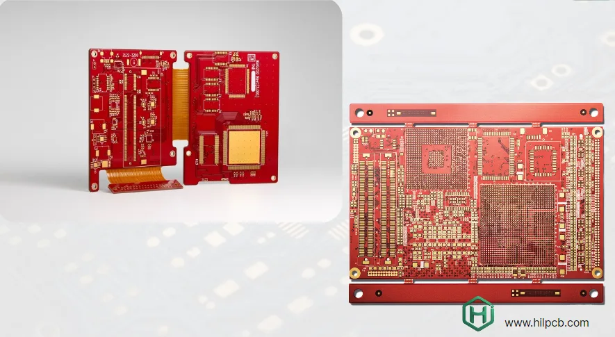
HILPCB supports HDI PCB manufacturing for density-driven designs using blind and buried vias, 1+N+1 and 2+N+2 build-ups, stacked or staggered microvias, and via-in-pad plated over. Published capability ranges include 3/3 mil standard and 2/2 mil advanced trace/space, plus 0.10 mm standard and 0.05 mm advanced laser holes; the buildable combination depends on copper, material, panel, thickness, and reliability requirements.
The useful first step is not choosing the smallest advertised feature. HILPCB can review BGA escape, stack symmetry, microvia spans, fill and planarization, sequential lamination count, impedance, inspection coupons, and assembly constraints before quotation. If microvias are unnecessary, a simpler multilayer PCB may be the lower-risk answer.
FAQ
What does 1+N+1 mean in an HDI PCB?
It means one sequential build-up layer is added to each side of a central N-layer core. The outer build-up layers commonly use laser microvias to connect to the adjacent core layers.
Are all microvias laser drilled?
Laser drilling is the dominant process for modern HDI microvias, but IPC-2226 covers multiple via-formation methods. The drawing should specify the required finished structure and let the approved fabrication process define formation details.
Are stacked microvias less reliable than staggered microvias?
Stacked structures place interfaces in one vertical column and therefore demand strong fill, registration, and qualification controls. Staggering often reduces stacked-interface risk but consumes routing area. Reliability depends on the exact construction and process evidence, not the label alone.
Does HDI always improve signal integrity?
No. Short blind transitions can reduce stubs and parasitics, but poor reference-plane continuity, unsuitable material, narrow return paths, or badly located transitions can still degrade a channel. Validate the full interconnect.
What files are needed for an HDI PCB quote?
Send fabrication data, drill files, stack-up, via table, BGA/package information, impedance requirements, material and copper notes, IPC class, reliability tests, quantities, and delivery requirements. Assembly data should be included when via-in-pad or thin-board handling affects PCBA yield.
Get an HDI stack-up review
Send HILPCB the package map, preliminary stack-up, routing constraints, impedance targets, microvia spans, and reliability requirements. The review will determine whether the design needs standard multilayer, 1+N+1, 2+N+2, or a more advanced structure—and remove unnecessary build-up steps before they become cost and yield problems.