
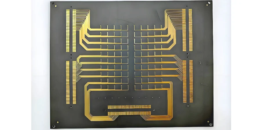
As 5G-Advanced evolves toward 6G, wireless communications are moving—at unprecedented speed—into higher frequency bands, wider bandwidths, and more complex system architectures. In this wave, the high-speed mmWave antenna array PCB is no longer just a carrier for components; it becomes a core determinant of the RF front-end (RFFE) system’s performance. As a baseband and fronthaul engineer responsible for eCPRI/O-RAN RU interfaces and clock synchronization, I know that every dB of loss and every picosecond of delay from baseband to antenna matters. Signals in mmWave bands (e.g., 28 GHz, 39 GHz, 60 GHz, and beyond) are extremely fragile, creating unprecedented demands on PCB material properties, design precision, and manufacturing processes. This article breaks down the key challenges in building a high-performance high-speed mmWave antenna array PCB and provides practical design and manufacturing strategies.
Filter and duplexer/multiplexer topology selection for mmWave antenna array PCBs
In dense spectrum environments, filtering and multiplexing act as the “gatekeepers” of link quality. For mmWave antenna arrays, how to implement efficient and compact filters and duplexers/multiplexers on the PCB is a primary design problem. This directly affects out-of-band Rejection, Insertion Loss, and isolation.
Topology trade-offs: from lumped elements to integrated waveguides
- Lumped-element (LC) filters: At lower frequencies, LC filters are popular due to flexibility and compactness. In mmWave, however, parasitics dominate and Q drops sharply—loss increases and performance often becomes unacceptable.
- Distributed filters: Based on transmission-line theory using microstrip/stripline, distributed filters are the mainstream in mmWave PCB design. By precisely controlling line length and geometry, you can achieve the needed response. The downside is that physical size scales with wavelength; even at lower mmWave (e.g., 28 GHz) they can still consume significant PCB area.
- SAW/BAW: Surface acoustic wave (SAW) and bulk acoustic wave (BAW) filters, with very high Q and miniature packages, dominate Sub-6GHz. While mmWave usage is still being explored, integrating them as discrete devices on antenna array PCBs raises complex interconnect and impedance-matching challenges with the PCB substrate.
- Substrate Integrated Waveguide (SIW): SIW builds two rows of plated vias inside the PCB dielectric to emulate the EM propagation of a metal waveguide. It combines waveguide-like high Q/low loss with planar integration, making it ideal for high-performance mmWave bandpass filters—especially in antenna feed networks.
In practice, topology selection is a balance across performance, size, and cost. For example, a complex phased-array antenna may use SIW filters in the feed network for minimum loss, while integrating compact BAW devices at specific TX/RX nodes. One effective mmWave antenna array PCB cost optimization approach is to use the best-fit hybrid topology per functional module.
High-frequency device integration: parasitics and precision assembly
In mmWave, even tiny physical structures can act like unintended “antennas” or “reactors”. High-density integration of PA, LNA, switches, and phase shifters on the antenna array PCB is the ultimate test of design and manufacturing.
Suppressing parasitics
Device packages (BGA/QFN), pads, vias, and interconnect traces introduce non-negligible parasitic inductance and capacitance. These parasitics alter impedance, create reflections, worsen insertion loss, and can even trigger self-oscillation.
- Grounding: A low-impedance, continuous ground plane is the foundation. Dense ground-via arrays under and around devices provide the shortest return path—critical for strict mmWave antenna array PCB impedance control.
- Via optimization: A signal via is effectively an inductive segment; its length (PCB thickness) introduces noticeable phase shift and loss at mmWave. Back-drilling to remove excess stub, or using HDI Microvias, are effective ways to reduce parasitics.
- Isolation: To prevent coupling between antenna elements and between RF channels and digital control lines, use ground isolation strips, Via Fencing, and sufficient physical separation.
Precision assembly processes
Precision assembly directly impacts mmWave performance. HILPCB’s prototype assembly service can meet the strict precision and reliability requirements of mmWave products.
- Soldering quality: Accurate solder paste printing, placement accuracy (X/Y/Z and rotation), and reflow profile control must reach micron-level standards. Joint voiding or component offset can severely impact impedance matching and thermal performance.
- Underfill: For BGA devices, underfill improves mechanical reliability, but materials must have ultra-low Dk/Df to avoid degrading RF performance.
📡 mmWave PCB high-frequency assembly: an ultra-precision closed loop (24GHz - 77GHz)
Review mmWave-sensitive devices with a focus on pad compensation and anti-pad/keepout design. Calibrate how solder mask opening (Solder Mask Opening) affects edge impedance to keep antenna-feed geometry aligned with simulation models.
Use laser-cut Step Stencil and automated SPI monitoring. Control micron-level solder paste Volume consistency to prevent parasitic capacitance from excess paste or impedance discontinuities from insufficient paste.
Use pick-and-place equipment with a high-performance vision system to precisely place 01005 components and fine-pitch BGA. Align solder balls with RF pad centerlines to eliminate signal loss caused by mechanical offset.
Run vacuum reflow under nitrogen. Force microbubbles out of BGA joints and push void rate to the limit (<5%), ensuring physical integrity and thermal stability on ultra-high-frequency signal paths.
100% coverage using 3D AOI and X-Ray CT. Quantify BGA joint coplanarity and internal structure to prevent any risk of shorts, cold joints, or voiding.
SI essentials: insertion loss, isolation, and group delay optimization
Signal Integrity (SI) is a core metric for high-speed mmWave antenna array PCB performance. At mmWave, every centimeter of transmission brings meaningful attenuation—so details matter.
- Reducing insertion loss
- Dielectric loss: The main contributor to total loss. Use ultra-low Df RF laminates, such as Rogers PCB materials or PTFE-based composites. Dk/Df must remain stable across the operating band.
- Conductor loss: Driven by Skin Effect and conductor surface roughness. At mmWave, current flows in an extremely thin surface layer. Use smoother VLP/HVLP copper foil and surface finishes such as ENEPIG that do not increase roughness to reduce conductor loss.
- Improving isolation High isolation (high Rejection) means less crosstalk and interference. Beyond layout isolation techniques, optimizing filter design for steeper roll-off and deeper out-of-band suppression is key.
- Controlling group delay Group Delay describes timing differences across frequency components. For wideband modulation such as OFDM in 5G/6G, strong group-delay ripple can cause severe ISI and reduce data rate. Filter and matching networks must keep group delay flat across the passband, which requires advanced EM simulation to co-optimize the full link—including traces, vias, and components.
Accurate mmWave antenna array PCB impedance control is the foundation for all of the above. Tools such as HILPCB’s impedance calculator (Impedance Calculator) help predict and control transmission-line impedance early in design.
From design to mass production: S-parameter consistency and de-embedding validation
Great simulation results mean little if they cannot be reproduced in real hardware. A rigorous mmWave antenna array PCB validation flow is the last—and most critical—line of defense.
S-parameter measurement and de-embedding
S-parameters are the standard language for RF networks. Using a VNA to measure a DUT’s S-parameters (e.g., S11 return loss, S21 insertion loss) provides a direct performance view. At mmWave, fixtures, probes, and cables introduce loss and reflections; De-embedding is required to remove these effects from results.
- TRL/LRM calibration: Thru-Reflect-Line (TRL) and Line-Reflect-Match (LRM) are two accurate on-board calibration methods. By fabricating calibration standards (thru, reflect, line) on the same PCB, you can build a precise calibration model and “move” the reference plane to the DUT ports, obtaining true S-parameters.
Ensuring mass-production consistency
Moving from a few prototypes to mmWave antenna array PCB mass production at scale requires extreme process control.
- Material consistency: Keep Dk, Df, and thickness variation of laminates within tight tolerances across lots.
- Process control: Apply strict SPC on critical steps such as etching, lamination, and drilling to keep line width/spacing and dielectric thickness highly consistent.
- In-line testing: Integrate ATE to sample or 100% test key RF metrics, ensuring every shipped high-speed mmWave antenna array PCB meets spec.
Successful mmWave antenna array PCB validation verifies not only the design, but also manufacturing robustness—laying the foundation for a smooth ramp to volume.
Key points for mmWave PCB validation
- Accurate fixture design: the fixture must be a 50Ω environment and provide stable, repeatable connections.
- Precision calibration standards: manufacturing accuracy of TRL/LRM standards directly determines de-embedding accuracy.
- Probe-contact reliability: use high-quality mmWave probes (e.g., GSG) and ensure consistent contact across measurements.
- Environmental control: temperature and humidity affect dielectric behavior; test in a controlled environment.
- Simulation-to-measurement correlation: compare measured S-parameters against simulation, analyze differences, and feed findings back into design and process iteration.
Cost vs. performance: material and process trade-offs for mmWave PCBs
Maximum performance often comes with high cost. Under commercialization pressure, mmWave antenna array PCB cost optimization becomes as important as the technical design.
Smart material selection
- All high-end materials: pure PTFE or ceramic-filled hydrocarbon laminates offer the best RF performance, but are expensive and harder to process.
- Hybrid lamination stackups: the most popular cost-optimization approach today. Use expensive low-loss materials only on the RF layers that carry mmWave signals, while using lower-cost standard FR-4 or High-Tg FR-4 for digital control, power, and ground layers. This High Frequency PCB approach requires careful handling of material bonding, lamination, and drilling across dissimilar materials.
- Emerging materials: the industry continues to develop new laminates with performance close to premium materials but lower cost and better manufacturability—expanding cost-optimization options.
Balancing process complexity and lead time
Processes like backdrill, buried/blind vias, and fine-line control increase manufacturing cost and cycle time. Engage closely with your PCB manufacturer early, understand process capability, and avoid over-design. For mmWave antenna array PCB quick turn, a partner with a mature process platform and fast engineering response is critical—they can help you avoid bottlenecks early, balancing performance requirements and time-to-market. From mmWave antenna array PCB quick turn prototypes to mmWave antenna array PCB mass production, cost awareness across the full flow is essential for commercial success.
Power integrity and thermal management: keeping mmWave arrays stable
A stable and reliable high-speed mmWave antenna array PCB needs not only perfect RF paths, but also strong “back-end support”: a robust PDN and thermal-management system.
Power Integrity (PI)
The many PA stages in mmWave arrays can demand huge transient current during TX. A poorly designed PDN can create rail noise and voltage droop, modulate RF signals, degrade EVM, and even cause system failure.
- Low-impedance PDN: Use wide power planes, plane capacitance, and extensive decoupling to build a low-impedance path from the power module to PA chips.
- Well-placed decoupling capacitors: Place decoupling capacitors of different values as close as possible to PA power pins to filter noise across frequency ranges.
Thermal management
PA efficiency is often limited; most electrical power becomes heat. In compact arrays, high heat density is a severe challenge.
- Thermal paths: Use dense thermal-via arrays under PA chips to conduct heat quickly to backside ground layers or heatsinks.
- Enhanced thermal processes: For very high power, use Heavy Copper PCB to improve lateral conduction, or use Coin-in-PCB copper coin technology to embed a solid copper slug under the chip for the lowest thermal-resistance path.
Effective thermal management keeps devices within safe temperatures and also avoids Dk/Df shifts driven by heat—helping maintain stable RF performance.
FAQ
Why is a mmWave antenna array PCB harder than an ordinary RF board?
Because it must solve beamforming density, phase consistency, feed-network loss, isolation, and manufacturing tolerance at the same time. At mmWave frequencies, even small dimensional errors, dielectric variation, or copper roughness changes can shift impedance and phase enough to reduce array gain and degrade EVM.
What matters most when selecting materials and stack-up for a mmWave antenna array PCB?
The key is to start from channel loss, phase stability, and thermal behavior together instead of choosing material by brand name alone. Designers usually need low-loss laminates, tightly controlled dielectric thickness, stable Dk/Df over temperature, and a stack-up that keeps RF paths short while still supporting grounding, shielding, and power delivery.
Why are PDN and thermal design directly tied to RF performance?
Because PA current transients and self-heating do not stay isolated in the power domain. Rail noise, voltage droop, and temperature rise can all modulate RF behavior, shift phase, change amplifier efficiency, and increase calibration difficulty, so PI and thermal design are part of the RF design problem rather than a downstream afterthought.
What should be validated before moving from mmWave prototypes to volume production?
Teams should validate impedance and phase consistency, insertion loss, antenna or feed-network behavior, thermal rise, and repeatability across panels and lots. It is also important to confirm that the chosen fabrication flow, test fixtures, and calibration method can scale without creating a gap between quick-turn prototype performance and mass-production yield.
Conclusion
Building a successful high-speed mmWave antenna array PCB is a multi-disciplinary system engineering effort spanning EM theory, materials science, precision manufacturing, and RF testing. From topology selection and SI design up front, to precision manufacturing and strict validation downstream, every step is challenging. Designers must carefully trade off loss, isolation, thermal performance, cost, and reliability.
As 6G explores higher THz bands, these challenges will become even tougher. Staying ahead requires continuous innovation from engineers—and strong partners like HILPCB with deep technical expertise and advanced manufacturing capability. With close collaboration, we can turn complex design blueprints into high-performing hardware, whether for mmWave antenna array PCB quick turn prototypes or mmWave antenna array PCB mass production deployments—building a solid hardware foundation for a fully connected future.