
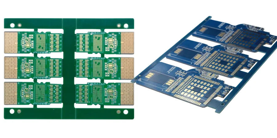
As data centers evolve at unprecedented speed, optical modules—often described as the “capillaries” of network infrastructure—directly determine data-flow efficiency and reliability. At the heart of the receive path, the high-speed TIA/LA receiver board is where opto-electrical conversion happens: it hosts the transimpedance amplifier (TIA) and limiting amplifier (LA), and it is the convergence point for high-speed SI, precise thermal management, and complex power distribution. As an engineer focused on TEC control and thermal design, I know that every mm² of placement and every thermal path can decide whether a module succeeds or fails. From a thermal-and-power engineer’s viewpoint, this TIA/LA receiver board guide breaks down design challenges under MSA constraints, hardware/software co-design, and the key controls that matter during manufacturing—so you can meet next-generation data center requirements.
How MSA form factors shape thermal/mechanical/electrical constraints
MSA standards define form factor, electrical interfaces, and thermal expectations for modules such as QSFP-DD, OSFP, and COBO. Standardization brings interoperability—but also imposes strict boundaries on high-speed TIA/LA receiver board design. As data rates move from 400G to 800G and even 1.6T, power density rises sharply, and the compact MSA envelope becomes the first challenge for thermal engineers.
1. Thermal constraints: In only a few cubic centimeters (e.g., QSFP-DD), the module must integrate lasers, modulators, TIA/LA, and DSP; total power can exceed 20 W easily. TIA/LA are high-gain, high-bandwidth analog devices and are extremely sensitive to operating temperature. Drift directly impacts gain, bandwidth, and noise figure—and thus receiver sensitivity.
- TEC integration and control: DWDM designs often integrate a thermoelectric cooler (TEC) for wavelength control. TEC itself is a power source; control efficiency, response speed, and its TIA/LA receiver board layout directly affect system energy efficiency and temperature-control precision. The PCB must provide strong thermal paths for the TEC controller and its power MOSFETs while preventing local hot spots from coupling into nearby high-speed routing.
- Thermal path design: Heat conduction from TIA/LA to the module shell must be engineered. This commonly involves high-conductivity TIM, embedded copper coins, or heat pipes. PCB substrate selection matters as well—for example, using High Thermal PCB materials or ceramic substrates in critical zones to improve vertical conduction.
2. Mechanical and electrical co-constraints: MSA mechanical tolerances are tight; PCB warpage and connector position accuracy must be controlled.
- Mechanical tolerances: Alignment between the PCB and the optical sub-assembly (OSA) directly affects optical coupling efficiency. Low-CTE substrates (Rogers, ceramics) help keep dimensions stable across operating temperature ranges (typically 0°C to 70°C), reducing thermally induced misalignment.
- Electrical isolation: In limited PCB area, high-speed differential pairs, low-speed control buses (I2C/MDIO), and multiple power rails are densely interleaved. TIA/LA receiver board layout must enforce strict isolation to keep digital noise from coupling into sensitive analog receive paths. Multilayer stackups enable region partitioning and shielding via carefully designed ground and power planes. HILPCB’s experience in Multilayer PCB fabrication supports complex stackups and tight impedance control to meet these constraints.
High-speed signal integrity: core challenges in TIA/LA receiver board routing
At 56 Gbps/lane and up to 112 Gbps/lane (PAM4), every trace segment on a TIA/LA receiver board behaves like a microwave transmission system. SI issues—loss, reflections, and crosstalk—are among the hardest challenges.
- Impedance control and matching: From photodiode (PD) to the TIA input, and from LA output to DSP, the channel impedance must be tightly controlled at 50 Ω (single-ended) or 100 Ω (differential). Any discontinuity (vias, connectors, package transitions) causes reflections, increasing jitter and BER. Accurate TIA/LA receiver board routing relies on 3D EM simulation to optimize trace width, dielectric thickness, and reference-plane integrity.
- Insertion loss: Dielectric and conductor loss attenuate HF signals. Selecting Ultra-Low Loss laminates is the first lever. Additional TIA/LA receiver board best practices—short routing, avoiding sharp corners, using smoother copper foils (VLP/HVLP)—also improve channel quality.
- Via design: Vias are unavoidable discontinuities in multilayer boards. Unoptimized vias create parasitic L/C; via stubs can resonate and severely degrade HF performance. Backdrilling removes stubs; blind/buried vias (HDI) shorten transitions and improve dense-area routing. HILPCB’s High-Speed PCB services support backdrill and HDI to enable high SI performance.
📡 TIA/LA receiver board: end-to-end engineering execution matrix
A standardized design path from weak-signal detection to high-bandwidth data recovery
| Design phase | Core tasks and deliverables | Key engineering considerations |
|---|---|---|
| 01. Requirements and architecture Data rate, MSA, power budget |
|
Thermal-resistance analysis of packages; SI model estimation for BGA/Wire-bond transitions; initial IR-drop estimate for power rails. |
| 02. Multi-physics simulation CFD / SI / PI co-simulation |
|
Material selection: Ultra-Low Loss laminates (M8/M7N); stackup symmetry to control warpage; PDN resonance suppression. |
| 03. Placement and routing Precision Routing |
|
Isolation: isolate power ground from sensitive TIA input return; control high-speed via stub; verify return-path impedance continuity. |
| 04. Manufacturing and engineering collaboration DFM / DFA / Quality |
|
Hold impedance tolerance to ±5%; lamination shift impact on differential phase; X-Ray inspection standard for critical BGA joints. |
| 05. Test and closed loop EVT / DVT / BER |
|
Thermal stability: sensitivity drift across temperature; host-platform compatibility; long-term reliability (HALT/HASS). |
For TIA/LA boards that are extremely sensitive, HILPCB provides ±3% impedance tolerance control and 2 mil laser depth-controlled backdrill. With early DFM collaboration, we help complex receiver circuits keep peak performance while achieving high first-pass yield at volume.
CMIS diagnostics and manageability: key points for hardware/software co-design
CMIS is the “brain” of modern pluggable optics. It defines a standard register map that allows the host to monitor state, control functions, and run diagnostics. high-speed TIA/LA receiver board design must provide solid hardware foundations for CMIS.
- Sensor integration: CMIS requires real-time monitoring of internal temperature, power-rail voltages, laser bias currents, and received optical power. That drives careful placement of temperature sensors, voltage monitors, and ADCs. From a thermal perspective, the temperature sensor should be near key heat sources (TIA/LA) to provide accurate feedback for over-temp alarms and fan control.
- Hardware alarms and interrupts: Include comparator circuits to trigger alarm/interrupt signals when monitored parameters exceed thresholds. This protects modules from permanent damage even when software polling is delayed.
- Data path: Monitoring data is collected over I2C or MDIO to the module MCU, then formatted per CMIS. Keeping these acquisition circuits clean in SI and power noise is essential.
I2C/MDIO isolation, integrity, and placement considerations
Although I2C/MDIO are low-speed, their routing can be challenging on a TIA/LA receiver board packed with high-speed digital and sensitive analog.
- Noise coupling: I2C/MDIO can pick up noise from high-speed lanes or switch-mode power. Route away from major noise sources, preferably on a dedicated layer, and shield with ground traces.
- Pull-ups and termination: Correct pull-up selection and placement matter for rise time and logic levels. Place resistors close to the receiver side for best signal quality.
- Bus isolation: In hot-plug or multi-master cases, use I2C isolators/buffers to improve robustness. Place them carefully with low-impedance power/ground connections.
A strong TIA/LA receiver board treats these “slow” management channels with the same discipline as high-speed nets so the module’s “nervous system” stays stable.
🎯 Core design sign-off: TIA/LA receiver optimization rules
Ensure signal determinism and thermal stability for 400G+ systems under extreme conditions
Key action: No after-the-fact patching. Run CFD thermal-fluid simulation during placement. For TIA/LA devices sensitive to temperature drift, build dedicated Thermal Via arrays to keep junction temperature (Tj) in the linear region and prevent gain degradation from overheating.
Key action: TIA is extremely ripple-sensitive. Use low-ESR/low-ESL decoupling matrices (e.g., 01005 capacitors). Keep power planes continuous and do not route high-speed signals across splits to eliminate induced transient noise.
Key action: Build a continuous Reference Plane. For mixed-signal A/D zones, apply “partition but don’t split” grounding: control return paths via single-point ties or ferrite beads, preventing ground bounce from disturbing weak signals.
Key action: Lock the process window with HILPCB early. Confirm Any-layer HDI via-stack capability, minimum Solder Mask Dam, and Dk stability of HF laminates so specs maintain high CPK in volume.
For precision boards like TIA/LA receivers, we recommend low-loss PTFE materials with vacuum lamination to reduce void rate and improve vertical-transition stability for 112G+. With early DFM engagement, your design is born ready for mass production.
EEPROM/serial number management and manufacturing traceability
EEPROM is the module’s “ID card,” storing vendor info, part number, serial number, and CMIS configuration parameters (wavelength, power class, etc.). Traceability is the core of quality management and supply-chain control.
- EEPROM programming: During production, EEPROM on every TIA/LA receiver board must be programmed accurately using dedicated fixtures and programming tools. PCB design should reserve accessible programming interfaces (test pads or small connectors).
- Serial number management: Serial numbers enable Traceability. A robust MES assigns unique serial numbers and records production, test, and assembly data—including critical component lots and test results.
- Data integrity: EEPROM data must be correct; any errors can prevent recognition by host systems or cause abnormal behavior. Post-program verification is mandatory.
HILPCB’s Turnkey Assembly integrates PCB fabrication, component sourcing, programming, and testing into one flow, ensuring end-to-end traceability and reducing supply-chain management burden.
Compatibility testing and consistency validation flow
Even a perfect high-speed TIA/LA receiver board design is worthless if it cannot run stably across major switches and routers. Compatibility testing is the final—and one of the most critical—gates before release.
- Electrical compliance: Verify the electrical interface meets MSA requirements such as SFF-8636 or CMIS pin functions, voltages, and timing, using oscilloscopes, network analyzers, and protocol analyzers.
- Software/firmware compatibility: Validate that CMIS/EEPROM mapping is parsed correctly by host systems from different vendors. This requires extensive plug/unplug testing on real equipment to confirm correct identification and parameter readout.
- Stress and abnormal-condition testing: Under temperature extremes and supply variations, test performance and stability. Simulate abnormal events such as fiber hot-plug and rapid link toggling to validate fault tolerance and recovery.
Following TIA/LA receiver board best practices is a prerequisite to passing these tests—especially robust power filtering, strong ESD protection, and careful handling of all interface signals.
🚀 HILPCB: vertically integrated assembly + full-function test solution
From precision SMT to end-to-end MES traceability, delivering industrial-grade assurance for optical products
Specs: Advanced lines support 01005 (0402 metric) micro components and 0.3 mm pitch BGA. Nitrogen reflow (N2 Reflow) significantly reduces void rate and oxidation risk.
Quality loop: Integrate 3D-AOI, in-line X-Ray, ICT, and FCT. Provide 100% optical inspection for optical-module assemblies, ensuring no shorts/no cold joints under BGA and meeting high-bandwidth reliability targets.
Customized: Automated in-line/off-line programming for EEPROM, MCU, and DSP. High-precision calibration ensures wavelength, output power, and extinction ratio meet MSA requirements and customer private protocols.
Supply-chain security: A complete MES enables board-level traceability from raw-material lots and operators to test results. Detailed DHR reports help customers handle FDA/medical and automotive-grade audits.
With HILPCB’s integrated fabrication + assembly capability, you reduce multi-vendor coordination. From Gerber confirmation to fully functional delivery, we can save 30%+ on prototype and iteration cycles.
FAQ
Why are MSA limits such a big challenge for a TIA/LA receiver board?
Because optical modules keep moving to higher data rates and power density while the form factor stays almost fixed. That leaves very little room for routing, cooling, and component placement.
How is the thermal path of a TIA/LA receiver board usually optimized?
Designers typically combine close coupling to the metal housing with thermal interface materials, dense thermal-via arrays, and layout isolation from hot devices such as DSPs or lasers.
Why does the receiver board need tight hardware-software coordination?
The onboard MCU often manages parameter tuning, power sequencing, and alarm monitoring. Without that coordination, the module is much harder to keep stable across changing temperatures and link conditions.
What must be verified for CMIS and host compatibility?
Teams need to verify EEPROM and CMIS data accuracy, electrical compliance with the target standards, interpretation by different host systems, and behavior under stress conditions such as hot-plug events and temperature swings.
Conclusion: system co-design enables excellence
In summary, high-speed TIA/LA receiver board design is a system-level co-design challenge across optics, electronics, thermal, mechanics, and software. Engineers must master high-speed circuit design, bring deep thermal knowledge, and understand standards like MSA and CMIS. From thermal-path optimization under MSA envelopes, to precision routing at Gbps rates, to hardware/software co-design for manageability—every link is challenging.
As your reliable partner, HILPCB leverages deep experience in high-speed, high-frequency, and high-thermal PCB manufacturing plus strong one-stop assembly/testing capability to help you overcome these challenges. We deliver not only a circuit board, but a validated, reliable, and highly manufacturable solution—helping your TIA/LA receiver board stand out in a competitive market and laying a solid foundation for next-generation efficient, intelligent data centers.