
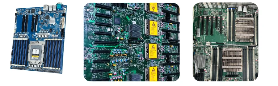
With the explosive rise of generative AI and large language models (LLMs), data centers are scaling compute demand at an unprecedented pace. As the core platform that carries GPUs, CPUs, and high-speed interconnect modules, industrial-grade AI server motherboard PCB design and manufacturing is facing challenges unlike any before. It is no longer merely a substrate for connectors and chips—it is the system’s “highway” and “power grid,” and its performance directly determines the throughput, stability, and scalability of an AI cluster.
As an engineer focused on rack-level interconnect systems in data centers, I know how critical the Backplane and Motherboard are in modern AI servers. From PCIe 5.0/6.0 Signal Integrity to multi-kilowatt power delivery and stringent DFM/DFX requirements, every step is a technical tradeoff. This article provides a comprehensive AI server motherboard PCB guide across connector selection, back-drilling strategy, materials science, and manufacturability—so you can navigate this complex domain. Partnering with a specialist manufacturer like Highleap PCB Factory (HILPCB) is key to turning these concepts into high-reliability products.
Why is stack-up design critical for AI server backplanes?
In AI servers, the backplane or motherboard is the nervous system connecting compute cards, storage modules, and network interfaces. Its Stack-up is the foundation of PCB performance, directly impacting Signal Integrity (SI), Power Integrity (PI), and thermal management. An optimized stack-up must strike a delicate balance among cost, performance, and manufacturability.
For a typical data-center AI server motherboard PCB, stack-up design should address:
Reference-plane integrity: High-speed differential pairs (e.g., PCIe, CXL) require continuous, unbroken GND or PWR reference planes. Any crossing of plane splits causes impedance discontinuities, leading to reflections and crosstalk, increasing Bit Error Rate (BER). In practice we plan at least 2–4 continuous GND layers to keep the return path short and clean.
Material selection: As signaling jumps from PCIe 4.0 at 16 GT/s to PCIe 6.0 at 64 GT/s (PAM4), traditional FR-4 can no longer meet loss targets. Choosing the right AI server motherboard PCB materials becomes critical. The industry typically selects loss classes based on link budget—Mid-Loss, Low-Loss (e.g., Megtron 4/6), and even Ultra-Low-Loss (e.g., Tachyon 100G). Lower Dk and Df reduce attenuation over the channel.
Interlayer symmetry and warpage control: AI server backplanes are large, often exceeding 20 layers. An asymmetric stack-up creates internal stress during lamination and thermal cycling, resulting in Warpage. This affects connector solder reliability and can even cause BGA failures. Keep the stack-up symmetric about the centerline and balance copper distribution.
Power/signal isolation: To minimize power noise coupling into high-speed signals, separate power layers from signal layers with effective GND shielding. A well-planned sequence such as
SIG-GND-PWR-GND-SIGprovides strong isolation and improves EMC.
A well-designed stack-up is half the battle. Early in the project, deep alignment with a High-speed PCB manufacturer like HILPCB—using its material library and process experience—helps avoid late-stage performance and build risks.
How do you tackle high-speed Signal Integrity challenges in the PCIe 5.0/6.0 era?
In the PCIe 5.0 (32 GT/s) and PCIe 6.0 (64 GT/s, PAM4) era, SI design has become the hardest part of industrial-grade AI server motherboard PCB development. Nyquist frequencies reach 16 GHz and beyond; even tiny impedance discontinuities get amplified and can destabilize the link.
Key strategies include:
Tighter impedance control: Differential impedance tolerance typically tightens from ±10% to ±7% or even ±5%. This demands precise etching and lamination control from the PCB manufacturer. On the design side, use 2D/3D field solvers to calculate trace width, spacing, and reference distances accurately.
Insertion Loss budget management: The end-to-end channel budget (CPU Root Complex to Endpoint) is limited, and PCB routing is a major contributor. Beyond low-loss materials, shorten routes, use wider traces where possible, and select ENIG over HASL to avoid worsening skin-effect behavior—reducing loss.
Crosstalk suppression: Higher routing density makes NEXT/FEXT more severe. Increase spacing between differential pairs (recommend >3W, where W is trace width), use orthogonal routing between adjacent signal layers, and strategically add GND Guard Traces in critical regions.
Advanced simulation and validation: At these speeds, rule-of-thumb design is not viable. Use professional SI tools (e.g., Ansys HFSS, Keysight ADS) for full-channel S-parameter simulation and analyze eye diagrams, jitter, and BER—so issues are found and fixed before fabrication.
PCIe generation: key Signal Integrity parameter comparison
| Parameter | PCIe 4.0 (16 GT/s NRZ) | PCIe 5.0 (32 GT/s NRZ) | PCIe 6.0 (64 GT/s PAM4) |
|---|---|---|---|
| Nyquist frequency | 8 GHz | 16 GHz | 16 GHz (Baud Rate) |
| Total channel loss budget | ~28 dB @ 8 GHz | ~36 dB @ 16 GHz | ~32 dB @ 16 GHz |
| Encoding | 128b/130b (NRZ) | 128b/130b (NRZ) | FLIT Mode (PAM4) |
| Sensitivity to material loss | Medium | High | Very high (more sensitive to linearity and noise) |
What are the optimization strategies for backplane connectors and via transitions?
In rack systems, signals travel through daughter cards, the backplane, and cables. Connectors and vias are the largest discontinuities along the signal path. Optimizing these transitions is essential to overall channel performance.
Via optimization strategy:
Via parasitic capacitance and inductance create impedance steps, while via stubs resonate at specific frequencies and can be devastating. Our core approach is “remove stubs, optimize geometry.”
Back-drilling: The most effective method to remove via stubs. From the opposite side of the PCB, a slightly larger drill removes the unused portion (stub). Precise depth control is the key. Experienced manufacturers like HILPCB can keep stub length within 10 mil, pushing resonance above 40 GHz—well beyond today’s operating bands.
Via structure optimization: Reducing Pad and Anti-pad dimensions lowers parasitic capacitance. In addition, placing Stitching Vias around the signal via provides a low-inductance return path and improves impedance continuity.
Connector selection and placement:
AI server backplanes typically use high-density, high-performance connectors such as Straddle-mount or Press-fit connectors.
Connector selection: Choose connectors designed for PCIe 5.0/6.0 with strong SI performance. Carefully review the vendor’s S-parameter models and import them into full-channel simulations.
Fan-out region design: The transition region from connector pins into PCB routing is difficult—dense routing increases crosstalk risk. Use “Dog-bone” fan-out or Microvia structures with HDI routing to keep each differential pair’s geometry as consistent as possible.
Achieving strict AI server motherboard PCB compliance means following electrical requirements from PCI-SIG and others—and executing every physical detail with discipline.
How do you design a robust Power Distribution Network (PDN) for hundreds of amps?
An AI server with 8 high-performance GPUs can exceed 5000 W peak power, meaning the motherboard must handle hundreds of amps. A robust PDN must deliver stable, clean power to all chips with extremely low IR Drop.
The core objective is ultra-low Target Impedance.
Layered power delivery and power planes: Allocate multiple solid power and ground layers for core rails (e.g., VCORE, VDDQ). Using Heavy Copper PCB (e.g., 3 oz or 4 oz copper) significantly reduces plane resistance and lowers IR Drop.
VRM placement and decoupling strategy: Place the VRM as close as possible to the load (e.g., GPU slots) to shorten the high-current path. Decoupling layout is the art of PDN design. Build a wideband decoupling network from low to high frequency based on capacitor value, ESR, and ESL—bulk electrolytic/tantalum for low-frequency transients, and large counts of MLCC around the chips to suppress high-frequency noise.
Power via design: A Via Farm for high-current paths must be sized for current-carrying capability and thermal effects to avoid overheating or fusing due to excessive current density.
PI simulation analysis: With professional PI tools, perform DC IR Drop and AC impedance analysis. This reveals weak spots early—such as current bottlenecks or impedance peaks—so you can optimize proactively.
⚡ High-power PDN design & Power Integrity (PI) matrix
VRM and decoupling capacitors must sit close to the load device. By minimizing current loop area (Loop Area), you reduce parasitic inductance and suppress high-frequency voltage ringing driven by transient current.
Configure Heavy Copper (2oz-3oz) based on high-current demand. By widening planes and optimizing via arrays, keep IR Drop strictly within 3% of the core rail to prevent excessive local power loss.
Allocate dedicated continuous planes for key rails. Combine capacitor arrays across packages (0201/0402) and values to keep PDN impedance below Target Impedance (Z-target) from kHz through GHz.
Before mass production, execute full DC/AC PI simulation. Validate plane resonance modes and return-path integrity, then predict and optimize SSN (simultaneous switching noise) behavior.
What advanced thermal-management techniques are used in industrial-grade AI server PCBs?
Performance and heat are inseparable. On an AI server motherboard PCB, not only GPUs and CPUs are major heat sources—VRMs, high-speed SerDes, and even high-loss PCB routing generate substantial heat. Effective thermal management is a prerequisite for stable 24/7 operation.
Thermal path design: The PCB itself is part of the cooling system. Dense Thermal Vias under hot components conduct heat quickly into internal ground and power planes. These large copper planes act as heat spreaders to distribute heat more evenly.
High Tg materials: Industrial-grade applications require mechanical and electrical stability at elevated temperatures. Using High Tg PCB materials (Tg > 170°C) improves heat resistance and reduces the risk of delamination or softening.
Embedded cooling techniques: For extremely high power density regions, use more advanced methods. For example, Copper Coin technology embeds a solid copper block in the PCB, directly contacting the heat source and conducting heat efficiently to a heatsink on the opposite side.
Thermal Simulation: Early in design, build a thermal model of the PCB, input component power data, analyze temperature distribution, identify hotspots, and optimize placement and cooling—keeping all components within safe operating limits.
How do DFM/DFX ensure manufacturability and reliability for AI server backplanes?
A theoretically perfect AI server motherboard PCB design is still a failure if it cannot be manufactured economically, efficiently, and at high yield. The gap between design and manufacturing must be bridged through DFM (Design for Manufacturability) and DFX (Design for Excellence).
AI server backplane complexity shows up in:
- Extra-large size: often exceeding 20 x 20 inches.
- Very high layer counts: typically 20–30 layers or more.
- High Aspect Ratio: board thickness to minimum drill diameter can exceed 15:1, challenging plating processes.
- Fine lines: 3/3 mil (trace/space) is common.
DFM reviews focus on:
- Drilling and plating: verify minimum hole size and Annular Ring against manufacturer capability, and plating uniformity for high Aspect Ratio holes.
- Etching: evaluate trace/space and impedance-control tolerances for process stability.
- Lamination alignment: interlayer registration accuracy directly impacts via reliability.
- Solder mask and surface finish: verify Solder Mask Bridge precision so high-density pins (e.g., BGA) do not bridge.
Working with a manufacturer like HILPCB—backed by strong engineering capability—enables free DFM analysis early. Their engineers provide capability-driven recommendations (e.g., via sizing, copper clearance adjustments), significantly improving yield, lowering cost, and accelerating time-to-market without sacrificing performance. That is a key value this AI server motherboard PCB guide aims to emphasize.
HILPCB advanced manufacturing capabilities at a glance
| Manufacturing parameter | Capability range | Value for AI server PCBs |
|---|---|---|
| Maximum layer count | 64 layers | Meets complex routing and power-plane partitioning needs |
| Maximum board thickness | 10.0 mm | Supports high-layer-count and heavy-copper designs for higher rigidity |
| Minimum trace/space | 2.5/2.5 mil | Enables high-density interconnects and advanced packaging |
| Maximum Aspect Ratio | 18:1 | Ensures reliable deep-hole plating in thick boards |
| Impedance control accuracy | ±5% | Meets high-speed interface requirements such as PCIe 5.0/6.0 |
What are the key compliance and test standards for AI server backplane PCBs?
For data-center AI server motherboard PCB products, reliability and compliance are non-negotiable. Boards must pass rigorous testing and certifications to ensure long-term stable operation in harsh data center environments.
IPC standards: IPC-6012 is the baseline. For high-reliability server products, IPC Class 3 is commonly required. Class 3 sets stricter requirements on conductor width, annular rings, plating quality, and more.
Impedance testing: Every production lot must be verified via TDR characteristic-impedance testing to confirm compliance with design targets (e.g., 85 Ω or 100 Ω). The report is a key document for AI server motherboard PCB compliance.
Reliability testing: Samples should pass environmental and mechanical stress tests, including:
- Thermal Shock: simulates rapid temperature changes.
- Temperature Cycling: evaluates failures from CTE mismatch across materials.
- PCT: evaluates moisture resistance.
- CAF testing: evaluates insulation reliability under high temperature/humidity and high electric-field gradients.
Micro-section analysis: Cross-sectioning under microscopy checks via plating quality, inner-layer interconnect reliability, and defects such as delamination or voids.
How do you choose the right AI server motherboard PCB manufacturer?
Selecting the right manufacturing partner is the last—and most critical—step to success. A strong AI server motherboard PCB manufacturer should offer:
- Deep technical expertise: more than a factory—a technical advisor that understands SI/PI and thermal intent and provides constructive DFM feedback.
- Advanced equipment and processes: capability for high-layer-count, high Aspect Ratio, fine-line builds, plus back-drilling and advanced processes such as embedded resistors/capacitors.
- Robust quality systems: certified under systems such as ISO 9001 and IATF 16949, with complete test equipment and procedures to ensure every board meets spec.
- Proven industry experience: successful cases in data center, server, and communications, and a deep understanding of Backplane PCB requirements.
- Flexible service and support: ability to scale from quick-turn prototypes to volume production, with engineering support available 24/7.
HILPCB brings these strengths together. With years of focus on high-speed and high-power PCB manufacturing, we provide an end-to-end solution—from design optimization and material selection to precision fabrication and strict testing.
Common Questions
Why is stackup design the foundation of an AI server motherboard or backplane?
Because the stackup sets the electrical and mechanical rules for the whole board. Reference-plane continuity, material loss class, layer symmetry, warpage control, and power-to-signal isolation all start there, so SI, PI, thermal behavior, and manufacturability rise or fall with the stackup.
Which structures create the biggest SI risks on PCIe 5.0 and PCIe 6.0 AI server boards?
The biggest risks usually come from long insertion-loss paths, connector launches, via stubs, dense pair-to-pair coupling, and weak impedance control. That is why AI server boards depend on low-loss materials, tight geometry control, backdrilling, spacing discipline, and full-channel simulation instead of rule-of-thumb routing.
What should a manufacturer prove before you trust it with an industrial-grade AI server motherboard PCB?
It should be able to demonstrate stable high-layer-count fabrication, heavy-copper PDN capability, high-aspect-ratio drilling and plating, ±5% impedance control, strong registration accuracy, and disciplined test coverage such as TDR, micro-section analysis, and environmental reliability checks. Without those capabilities, performance on paper will not survive production.
Conclusion
Designing and manufacturing a high-performance industrial-grade AI server motherboard PCB is a complex systems project that blends materials science, electromagnetics, thermodynamics, and precision process engineering. From ensuring PCIe 6.0 link Signal Integrity, to delivering stable power for multi-kilowatt systems, to maintaining long-term reliability in harsh data center environments—every link in the chain is challenging.
Success requires an integrated design mindset and close collaboration with an experienced manufacturing partner like HILPCB from day one. With early co-design, rigorous simulation validation, and DFM/DFX throughout, you can build the solid hardware foundation needed for the next wave of AI compute.
If you are launching a challenging AI server program—or want to optimize an existing AI server motherboard PCB design—contact our technical experts. We’re happy to share experience and provide end-to-end support from prototype to mass production.