
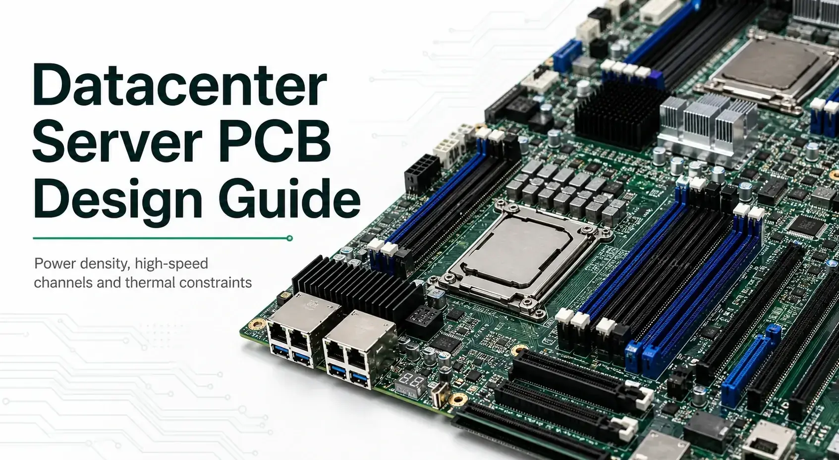
An IPU PCB is the board-level platform that connects an infrastructure processing accelerator to host PCIe, network, memory, management, power, and cooling interfaces in a server. IPU, DPU, and SmartNIC are overlapping vendor and market categories rather than universally interchangeable technical definitions, so a successful board begins with the selected silicon, card specification, and server boundary conditions—not a generic layer-count or material recipe.
Key Takeaways
- Translate workload and system architecture into interface, power, thermal, management, firmware, and mechanical budgets before choosing the stackup.
- Budget the complete high-speed channel: package, card traces, vias, connector, baseboard or riser, cable or module, and any retimer. A PCB-only simulation can miss the dominant loss or discontinuity.
- PCIe generation, Ethernet rate, layer count, laminate family, HDI structure, backdrill depth, impedance tolerance, and IPC class are project requirements—not universal properties of an “IPU PCB.”
- Select laminate and foil from loss, skew, fabrication, thermal, and cost analysis. Standard FR-4 is not automatically suitable or unsuitable because a board contains an IPU.
- Derive the PDN from rail-specific load steps, allowable droop, sequencing, connector/contact loss, telemetry, and cooling limits rather than one headline TDP value.
- Validate the actual card in its server airflow and pressure-drop environment, including heatsinks, VRMs, memory, connectors, and optical modules.
- Treat firmware inventory, FRU data, clock/reset mapping, power states, and pre-OS update behavior as hardware requirements when the platform specification calls for them.
- Connect each critical requirement to analysis, prototype evidence, production controls, system validation, and change triggers.
Contents
- What Is an IPU PCB?
- How Do Workloads Become Board-Level Budgets?
- Which Form Factor and Platform Requirements Matter?
- How Should the Complete High-Speed Channel Be Budgeted?
- When Do Low-Loss Materials, HDI, and Backdrilling Help?
- How Should the IPU Power Delivery Network Be Designed?
- How Do Thermal and Mechanical Constraints Change the PCB?
- What Management, Security, and Firmware Hardware Is Required?
- Which Failure Modes Should Be Reviewed Before Layout Release?
- How Should Prototype Evidence Become Production Control?
- What Should an IPU PCB RFQ Include?
What Is an IPU PCB?
Infrastructure accelerators move selected networking, storage, security, virtualization, and platform-management work away from the host CPU. Current commercial platforms may combine programmable processing, Ethernet interfaces, PCIe, memory, cryptographic or compression engines, storage offload, and a management subsystem. The board turns those silicon functions into a deployable server component.
The terminology needs care:
| Term | Useful working definition | Why the name does not define the PCB |
|---|---|---|
| NIC | A network interface between a host and a network | A NIC can be simple or highly programmable; the label does not reveal host lanes, port rate, memory, or power |
| SmartNIC | A NIC with programmable or fixed-function offload | Implementations range from modest offload cards to complex accelerator platforms |
| DPU | A vendor-defined data-processing accelerator that commonly combines compute, network, storage, and security functions | Architecture and packaging vary by vendor and product generation |
| IPU | A vendor-defined infrastructure-processing category focused on managing or accelerating platform infrastructure | The term does not mandate a form factor, layer count, interface generation, TDP, or cooling method |
The same silicon could appear on an add-in card, OCP NIC-style card, mezzanine, custom module, or server motherboard. Each implementation changes channel reach, power, keepouts, airflow, service, and validation. Use “IPU PCB” as a category, but use the actual platform specification as the engineering authority.
How Do Workloads Become Board-Level Budgets?
Jumping from “we need 200G networking” to “use an ultra-low-loss 20-layer board” skips the decisions that determine whether the design will work. Start with workloads and deployment constraints, then allocate board budgets.
Workload-to-board-budget matrix
| Workload or platform decision | Inputs to freeze | Board-level consequences | Evidence needed before release |
|---|---|---|---|
| Host offload scope | PCIe generation, lane count, bifurcation, host count, peer-to-peer paths, reset model | Connector pinout, routing topology, REFCLK/PERST distribution, retimer decision, sideband routing | End-to-end channel model, clock/reset timing review, enumeration and recovery test plan |
| Network ports | Port count, signaling rate, electrical/optical module, reach, FEC and protocol requirements | SerDes escape, cages/connectors, AC coupling, module power, thermal hotspots, management buses | Channel compliance plan, module compatibility matrix, worst-case thermal model |
| Storage offload | NVMe or network-storage interfaces, device count, topology, boot behavior | Additional PCIe lanes/switches, clocks, resets, power sequencing, hot-plug signals where applicable | Topology review, timing and recovery tests, firmware inventory requirements |
| Local memory and accelerators | Memory type, width, data rate, package escape, auxiliary accelerators | Dense fan-out, reference planes, skew constraints, PDN rails, placement and cooling limits | Vendor design-rule review, SI/PI simulation, memory training and stress plan |
| Security and isolation | Root of trust, secure boot, keys, debug policy, ownership boundary | Protected storage, strap control, tamper/debug access, update/recovery path, power-domain dependencies | Threat-linked hardware review, provisioning flow, recovery and lifecycle test plan |
| Management and service | BMC interface, telemetry, FRU, inventory, pre-OS update, field replacement | SMBus/I2C/MCTP or other sideband nets, EEPROM, sensors, isolation/muxing, service connector | Address map, power-state behavior, inventory/update test, field-service procedure |
| Deployment environment | Card form factor, inlet temperature, airflow direction, pressure drop, altitude, shock/vibration, service access | Outline and keepouts, heatsink retention, copper balance, stiffening, sensor placement, connector load | Mechanical tolerance analysis, CFD or thermal model, fixture and system validation |
This matrix prevents the stackup from becoming a proxy for unresolved architecture. A retimer may recover channel margin but adds power, firmware, clocks, sideband routing, latency, and cooling. Dense BGA escape may justify HDI, while different placement may avoid sequential lamination.
Which Form Factor and Platform Requirements Matter?
A card specification can drive more PCB requirements than the accelerator datasheet. Connector location, datum scheme, component keepouts, faceplate, airflow direction, hot-plug assumptions, shock/vibration, sideband ownership, and power-state behavior all affect placement and routing.
OCP NIC 3.0 Version 1.6.0 is a useful public example, not a universal IPU specification. It defines multiple card implementations and mechanical constraints; PCIe lanes, reference clocks, resets, and bifurcation controls; power states and slot power envelopes; management interfaces; temperature and power reporting; FRU content; firmware inventory/update behavior; PCIe electrical budgets; and thermal fixtures. Its primary connector definition supports up to PCIe Gen 5 at 32 GT/s, while its slot tables include several power classes rather than one “typical IPU power.” A custom accelerator card may use entirely different limits.
Before schematic release, build a platform interface control document that answers:
- Which revision controls the outline, connector, pinout, datums, keepouts, retention, and faceplate?
- Who supplies each rail, clock, reset, presence, wake, power-enable, power-good, and sideband signal, including multi-host or bifurcated mapping?
- What may operate in off, identification, auxiliary, programming, and main-power states, and what inventory/update functions must remain available?
- What airflow direction, inlet temperature, pressure drop, heatsink envelope, and server fan capability apply?
- What happens during insertion, removal, brownout, failed update, overtemperature, and host reset?
Do not call a card hot-swappable merely because its connector is field replaceable. Hot swap requires defined mechanics, inrush and isolation, sideband and firmware behavior, and system validation; some specifications leave parts of its implementation out of scope.
How Should the Complete High-Speed Channel Be Budgeted?
An IPU card may carry host PCIe, Ethernet SerDes, memory, clocks, management buses, and lower-speed control signals. Each interface needs its own topology and compliance target. The most important SI question is not “Can the PCB route 32 GT/s?” but “Does the complete channel meet the transmitter, receiver, connector, package, board, and system budgets with manufacturing variation included?”
Build an end-to-end channel model
For every critical link, document the path from die to die or die to module:
- transmitter package and breakout
- on-card traces, vias, AC-coupling components, connectors, and test structures
- baseboard, riser, cable, or optical-module electrical interface
- any retimer, redriver, switch, or mux
- receiver package and termination
Model insertion and return loss, crosstalk, mode conversion, skew, via resonance, plane transitions, connectors, and equalization. Include the Dk/Df method, copper roughness, etch, plating, glass weave, temperature, and fabrication tolerances. A nominal field-solver result is not production margin.
Preserve return paths through transitions
Layer changes need nearby return vias tied to the correct reference. Plane splits, voids, antipads, connectors, and BGA escape can force long return-current detours. Ground guard traces do not repair a broken reference path.
Decide retimers from the system budget
A retimer is justified when the passive channel lacks margin or topology demands lane conditioning. Place it so both segments meet their budgets, then account for clocks, rails, firmware, thermals, telemetry, reset, and recovery. It is not a late substitute for uncontrolled transitions.
Control the simulation models and record any substitute package or connector model and its uncertainty.
When Do Low-Loss Materials, HDI, and Backdrilling Help?
Material, layer count, and via technology should follow topology and loss analysis. A product name or “ultra-low-loss” is not a stackup specification; define construction, resin content, glass style, foil, thickness, impedance geometry, and substitution rules.
| Decision | Use it when | Do not assume | Evidence to request |
|---|---|---|---|
| Lower-loss laminate | Channel loss, Dk/Df stability, temperature, or reach requires it | Every fast interface needs the lowest-Df material on every layer | Frequency-dependent material data, roughness model, stackup field-solver report, coupon correlation plan |
| Low-profile copper | Conductor loss and roughness-induced phase behavior consume meaningful margin | A foil trade name alone predicts finished loss | Foil profile and treatment, etch/plating assumptions, insertion-loss coupon method |
| HDI/microvias | BGA pitch, escape density, placement, or layer transition strategy requires blind/buried structures | All IPU packages require any-layer HDI | Via structure, sequential-lamination count, capture pads, reliability qualification, registration capability |
| Backdrilling | A plated-through-hole stub creates unacceptable resonance or loss and the geometry permits controlled removal | Every high-speed via must be backdrilled | Finished residual-stub requirement, drill side, depth reference, keepout, coupon or section evidence |
| More layers | Routing, reference planes, PDN, shielding, copper balance, or breakout needs them | IPU boards must have 18–28 layers or more | Route study, plane allocation, press-cycle and material availability review |
Specify backdrilling by allowed residual stub and acceptance method, not only drill depth. Account for board thickness, dielectric variation, plating, drill-point geometry, registration, and drill side. Compare blind vias or different layer assignments when they solve the channel more reliably.
Geometric stackup symmetry alone does not prevent warpage when copper distribution, resin flow, component mass, or repeated lamination are unbalanced. Review actual copper density and assembly thermal profile.
For project-specific stackup and channel review, HILPCB can evaluate the submitted requirements through its high-speed PCB and HDI PCB workflows. Material availability, feature sizes, impedance acceptance, via structures, coupons, and inspection evidence must be confirmed in the quotation rather than inferred from this article.
How Should the IPU Power Delivery Network Be Designed?
A headline TDP cannot define the PDN. Accelerator cores, memory, SerDes, retimers, optics, management, and clocks have distinct current, transient, droop, sequence, sensing, and fault requirements.
Create a rail-by-rail power contract
For each rail, record:
- load voltage range, DC-drop allocation, steady/transient current, slew rate, and allowable droop
- target impedance or time-domain requirement over the relevant frequency range
- regulator topology/control model, remote-sense point, and decoupling assumptions with derating
- power-up, reset release, power-good, discharge, brownout, retry, and fault behavior
- connector/contact, protection, copper and via current-density, and hotspot limits
- telemetry accuracy, bandwidth, thresholds, calibration, and ownership
Place regulators from electrical and thermal analysis; proximity can conflict with heatsink keepouts, airflow, magnetics, BGA escape, and service. Remote sense needs a clean load reference. Neckdowns, antipads, connectors, and fuses may dominate otherwise broad planes.
Analyze DC drop and current density at worst-case copper and temperature, then simulate transients with realistic regulator, capacitor, package, and load models. Validate representative load steps, sequencing, brownout, faults, and thermal soak—not only room-temperature idle.
If FRU, recovery, presence, or telemetry operates from auxiliary power, prevent unpowered-domain leakage and back-powering. Verify cross-domain signals in every partial-power state.
How Do Thermal and Mechanical Constraints Change the PCB?
The PCB is one thermal-path segment. The package lid and heatsink normally remove most accelerator heat; the board spreads heat from terminals, VRMs, memory, retimers, and modules. Vias and planes cannot compensate for inadequate cooling.
Model the assembled card with:
- actual component power maps and operating modes rather than uniform board heat
- package thermal models, heatsink/TIM, retention load, flatness, and contact resistance
- optical or copper modules, cages, front-panel recirculation, and neighboring cards
- VRMs, inductors, memory, retimers, and local airflow shadowing
- server airflow direction, inlet temperature distribution, altitude, fan curve, impedance/pressure drop, and hot/cold aisle boundary conditions
- tolerances for dust loading, fan failure or degraded cooling where the system requirement includes them
OCP NIC 3.0 illustrates why the server context matters: it provides different hot-aisle and cold-aisle analyses and fixture guidance, and it expects card airflow requirements to be communicated in FRU data for relevant implementations. The lesson is not to copy its temperature curves into a custom design; it is to validate the card against the server's real airflow capability.
Review deflection under heatsink/connector loads, stiffeners, package warpage, solder strain, insertion, faceplate alignment, and shock/vibration. Keep mounting holes, metal hardware, and backplates within electrical-clearance and routing constraints.
Copper coins, metal regions, heat pipes, or liquid cooling are specialized options. Compare their manufacturability, CTE, flatness, serviceability, and validation burden with conventional heatsink/airflow solutions.
What Management, Security, and Firmware Hardware Is Required?
A card can pass traffic tests yet fail deployment because it cannot be inventoried, updated, recovered, or diagnosed. Include management hardware from the beginning.
Typical questions include:
- What identifies the board, silicon, memory, optics, and firmware before the host OS loads?
- Who owns FRU, sensors, update, boot status, logs, and recovery, and which functions survive on auxiliary power?
- How are sideband addresses assigned, isolated, multiplexed, and protected against a stuck device?
- Can an interrupted update recover without exposing an uncontrolled accelerator or network path?
- How are secure boot, provisioning, debug, manufacturing test, RMA, and decommissioning separated?
- Are straps and security-state pins defined through ramp, brownout, reset, and partial power?
Treat management buses as availability interfaces: calculate loading and pull-ups, control translation, and consider stuck-low isolation. Place sensors at the controlled hotspot or inlet and define telemetry accuracy from the platform contract.
Security extends beyond the PCB. The platform owner defines trust, provisioning, updates, and key custody; the supplier implements the contracted components, programming, serialization, and manufacturing controls. Fabrication alone does not make a platform secure.
Which Failure Modes Should Be Reviewed Before Layout Release?
Review cross-domain failures before constraints are embedded in dense layout; many escape checklists organized only by SI, PI, or thermal discipline.
| Failure mode | Why it escapes early review | Prevention or detection |
|---|---|---|
| Channel passes on card but fails in server | Connector, riser, baseboard, package, or module was omitted | Control one end-to-end model and allocate explicit loss/return-loss/skew budgets |
| Intermittent lane training | REFCLK/PERST mapping, bifurcation, reset timing, or power-good dependency is wrong | Interface-control review plus cold/warm reset and topology tests |
| Prototype passes, later lots lose margin | Material, foil, glass style, etch, plating, or stub changed | Controlled stackup, approved equivalents, coupons, lot records, change triggers |
| Rail droop during burst workload | Average current or bench load did not represent transient demand | Vendor load model, time-domain PI analysis, representative load-step test |
| Connector or via field overheats | Plane analysis ignored contact resistance, neckdowns, and local current crowding | Worst-case DC/thermal model and instrumented full-load test |
| Card throttles only in target rack | Open-bench cooling did not match inlet temperature, direction, pressure drop, or neighboring cards | System-level thermal fixture and representative server test |
| FRU or update unavailable during service | Management functions were tied to the main rail or blocked by an unpowered domain | Power-state matrix, back-power review, pre-OS inventory/update validation |
| Secure state becomes undefined on brownout | Strap, reset, key storage, or controller domains decay in the wrong order | Brownout and partial-power fault tests tied to security requirements |
| BGA or connector solder fatigue | Board deflection, heatsink load, CTE mismatch, or warpage was not modeled | Mechanical analysis, assembly profile review, strain/warpage evidence as required |
| Debug interface remains exposed | Manufacturing access was never transitioned to release state | Provisioning record, access-control test, release checklist, RMA procedure |
Assign an owner and closure evidence to each risk. “Checked” is not closure; a model revision, drawing note, test result, or approved waiver is.
How Should Prototype Evidence Become Production Control?
A prototype proves one configuration. Deployment requires margin across approved materials, fabrication variation, assembly, firmware, fixtures, server environments, and changes.
Prototype-to-deployment margin ledger
| Requirement | Model or analysis | Prototype evidence | Production control | System validation | Re-open when |
|---|---|---|---|---|---|
| PCIe/Ethernet channel | End-to-end S-parameters, loss, reflection, crosstalk, skew, equalization | Compliance or margin test with defined fixtures; coupon correlation | Controlled stackup/material/foil, impedance and loss coupons as contracted, backdrill evidence | Target server/riser/module interoperability and stress | Material, connector, package, layout, retimer firmware, fixture, or supplier changes |
| Rail voltage and transient | DC drop, current density, target impedance, transient simulation | Load-step, startup, brownout, fault, and thermal measurements | Copper/plating, components, placement, programming, inspection and functional limits | Representative accelerator workload and power-state cycling | Regulator, capacitor, connector, copper, firmware, load profile, or cooling changes |
| Thermal margin | CFD or compact thermal model with tolerance cases | Instrumented card in defined airflow fixture | TIM/heatsink/torque, sensor placement, assembly and inspection controls | Worst-case server slot, inlet, airflow and workload | Heatsink, TIM, module, fan policy, enclosure, component power, or placement changes |
| Management and recovery | State machine, address map, update/recovery analysis | Power-state, inventory, interrupted-update and bus-fault tests | Program/configuration verification, serialization, FRU and firmware records | BMC/pre-OS integration, field-replacement workflow | Controller, EEPROM, bus topology, firmware, security policy, or platform changes |
| Mechanical reliability | Tolerance, deflection, warpage, retention and vibration analysis | Fit, insertion, strain/warpage or environmental tests as required | Outline, thickness, stiffener, hardware, assembly profile, torque controls | Representative chassis installation and service cycles | PCB construction, package, heatsink, connector, chassis, or assembly-process changes |
The ledger makes change review concrete: a laminate is not equivalent if it changes loss, skew, pressing, expansion, or coupon correlation. Firmware is not software-only if it changes power states, equalization, thermal policy, or recovery.
Select inspection from actual risks. AOI, electrical test, microsection, TDR/loss coupons, X-ray, boundary scan, programming verification, and functional test answer different questions. Define sampling, limits, data, and acceptance in the purchase package.
IPC Class 3 is contractual, not automatic for every accelerator. Select IPC-6012, IPC-A-600, J-STD-001, and IPC-A-610 criteria from the reliability plan and contract, then add project criteria for channel, PDN, firmware, and thermal margin.
What Should an IPU PCB RFQ Include?
An actionable RFQ exposes risk before quoting. Gerbers plus “high-speed low-loss material” are not enough.
Architecture and platform
- accelerator, memory, retimer, switch, clock, regulator, connector, cage, and module part numbers with controlled datasheets/models
- card/form-factor specification and revision, outline, datums, keepouts, faceplate, retention, stiffener/backplate, heatsink/TIM, airflow direction, inlet conditions, and server slot constraints
- host/network/storage topology, lane mapping, bifurcation, clocks, resets, sideband buses, power states, hot-plug assumptions, and management ownership
- security, provisioning, firmware inventory/update, FRU, telemetry, recovery, debug-lock, serialization, and RMA requirements allocated to the PCBA process
PCB fabrication package
- ODB++/IPC-2581 or Gerber, NC drill, netlist, fabrication drawing, stackup, impedance table, material and foil specification, finished thickness, surface finish, solder mask, marking, panelization, and applicable IPC class/revisions
- controlled channel geometry, insertion-loss or coupon requirements, impedance acceptance, fiber-weave/skew controls where needed, backdrill side and residual-stub limit, via fill/cap/planarization, and HDI/sequential-lamination structure
- copper weights, current-critical regions, thermal structures, press-fit or connector requirements, mechanical tolerances, bow/twist or flatness requirements, and approved material-equivalence process
- required records: material certificates, stackup, impedance/TDR data, loss coupon data, microsections, backdrill evidence, electrical test, dimensional/visual reports, and lot traceability as applicable
Assembly and test package
- BOM with approved manufacturers and alternates, centroid, assembly drawings, stencil constraints, reflow limits, moisture-sensitive handling, underfill or TIM instructions, heatsink/fastener torque, and cleaning/coating requirements
- X-ray or other inspection criteria for hidden joints, press-fit requirements, programming/provisioning files, secure-data handling, boundary-scan/ICT/functional fixtures, golden units, limits, log format, and fixture ownership
- power-up sequence, current limits, rail measurements, firmware version, FRU content, identity/serialization, port/loopback tests, telemetry, sensor calibration, update/recovery, and debug-lock verification
- prototype, engineering validation, pilot, and production quantities; approved substitutions; deviation/rework authority; record retention; change notification; packaging; and delivery requirements
Evidence and responsibility
- requirement-to-test matrix with owners, sample sizes or 100% requirements, acceptance limits, report format, and nonconformance workflow
- system-level tests retained by the customer, including full-channel compliance, server interoperability, workload, thermal, security, firmware lifecycle, and regulatory validation
- explicit statement of which capabilities, tolerances, materials, inspections, tests, certifications, and lead times the supplier has confirmed for this exact build
HILPCB can review the fabrication, assembly, sourcing, and agreed test package through turnkey PCB assembly. The quotation should confirm the actual manufacturing route, material availability, tolerances, inspection/test coverage, evidence package, quality-system scope, quantities, and schedule.
Standards and Responsibility Scope
Common references may include the selected accelerator and connector vendor specifications; the applicable PCI Express Base and Card Electromechanical specifications from PCI-SIG; relevant IEEE 802.3 Ethernet clauses; OCP NIC 3.0 when that form factor is selected; IPC-2221 for generic PCB design; IPC-4101 for base-material specifications; IPC-6012 for rigid-board qualification and performance; IPC-A-600 for bare-board acceptability; J-STD-001 for soldered electrical and electronic assemblies; IPC-A-610 for electronic-assembly acceptability; and customer-specific server, security, environmental, and quality requirements. Confirm the applicable revisions and precedence in the contract.
The platform owner is responsible for architecture, interface budgets, security and firmware policy, system thermal/mechanical limits, reliability targets, standards selection, interoperability, and final-system validation. The PCB/PCBA supplier is responsible only for the fabrication, assembly, inspection, documentation, programming, and test scope accepted in writing. A PCB or PCBA build does not by itself certify PCIe or Ethernet compliance, workload performance, cybersecurity, server interoperability, field reliability, or OCP conformity.
Common Questions
What is an IPU PCB?
An IPU PCB is the board that integrates an infrastructure accelerator with host PCIe, network, memory, management, power, and cooling interfaces. Its exact requirements come from the selected silicon, form factor, server, and workload.
Are IPU, DPU, and SmartNIC the same thing?
Not universally. Vendors use the terms for overlapping infrastructure-acceleration products, but architectures and capabilities differ. Procurement and engineering documents should name the exact device and interfaces instead of relying on the category label.
How many layers does an IPU PCB need?
There is no fixed answer. Layer count follows BGA escape, interface topology, reference-plane needs, PDN, mechanical thickness, copper balance, and fabrication limits. A route and stackup study should determine it.
Does every IPU board need ultra-low-loss laminate?
No. Select materials from the complete channel loss and skew budget, temperature, construction, copper roughness, availability, and cost. Some layers or interfaces may justify lower-loss material while others do not.
Is backdrilling mandatory for PCIe Gen 5 channels?
No. Backdrilling is one way to reduce harmful plated-through-hole stubs. Use channel analysis to determine whether the stub consumes margin, then specify residual-stub and inspection requirements. Blind vias or a different layer transition may be better in some designs.
What should be validated before an IPU card moves beyond prototype?
Validate complete-channel margin, rail transients and power states, thermal behavior in the target server, management and firmware recovery, mechanical fit and loading, assembly quality, and repeatability under controlled production materials and processes.
Does every data center IPU PCB require IPC Class 3?
No. IPC class is selected by the product reliability plan and contract. Workmanship class also cannot replace design-specific SI, PI, thermal, firmware, security, or interoperability evidence.
What information does a supplier need to quote an IPU PCB accurately?
Provide the controlled fabrication and assembly data plus stackup/channel requirements, form-factor constraints, power and thermal conditions, BOM, programming, inspection/test plan, evidence package, quantities, and change-control rules.
Turn the architecture into explicit board budgets and evidence requirements, then request a HILPCB engineering review and quote for the defined PCB/PCBA scope.