
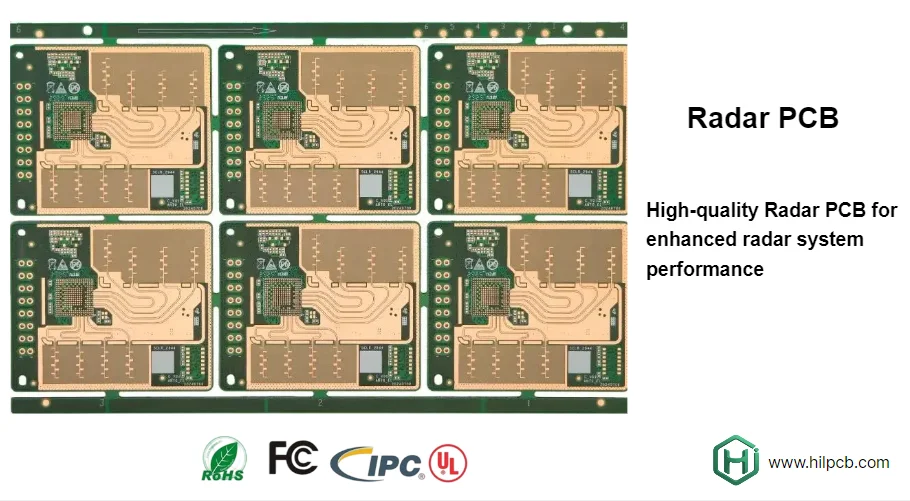
With the global wave of vehicle intelligence and electrification, Advanced Driver Assistance Systems (ADAS) and EV power systems have become two core technologies shaping the future of mobility. As a BMS (battery management system) design specialist, I know that in harsh automotive environments, the failure of any electronic component can lead to catastrophic consequences. The PCB that carries sensing, decision, and execution functions is therefore critical. This article focuses on low-loss ADAS radar PCB and, drawing from EV power PCB experience in high voltage, high current, and long-term reliability, discusses how to tackle these dual challenges in automotive electronics.
ADAS relies on sensors such as mmWave radar for precise perception. Even small attenuation of radar signals at high bands such as 77/79 GHz directly impacts detection range and accuracy. Therefore, low-loss ADAS radar PCB using low-loss materials and precision manufacturing is the foundation of system performance. Meanwhile, EV power systems such as BMS, OBC, and inverters demand extreme thermal capability, current-carrying capacity, and long-term reliability. These seemingly different applications converge on the same goal: maximum reliability and safety. This is a comprehensive ADAS radar PCB guide that blends the design essentials from both domains.
Common challenges for ADAS radar and EV power PCBs: efficient thermal structure design
Whether keeping an ADAS radar’s core MMIC stable or managing the massive heat from EV battery packs and power modules, efficient thermal management is key to performance and lifetime.
1. Hot-spot management for ADAS radar MMICs can generate concentrated hot spots at high speed. Rising temperature degrades performance, causes frequency drift, and may even lead to permanent damage. To remove heat effectively, low-loss ADAS radar PCB designs typically use:
- Thermal Vias: place arrays of plated vias under the chip pads to conduct heat quickly into inner/bottom ground/power planes.
- Coin Insertion: embed high-thermal-conductivity metal (copper/aluminum coin) into the PCB and contact the die area tightly to form an ultra-low thermal-resistance path.
- High-thermal materials: select higher-thermal-conductivity substrates such as MCPCB, especially suitable for radar modules integrating power devices.
2. System-level cooling for EV power PCBs EV power PCB thermal design is more system-oriented. Balance circuits on BMS boards, high-voltage sense resistors, and inverter IGBT modules are major heat sources. Common approaches include:
- Heat Spreader/Sink: use TIM to couple power devices to large aluminum/copper heatsinks.
- Cold Plate: for higher power density, actively cool with a cold plate containing internal coolant channels for excellent temperature control.
- Vapor Chamber (VC): use phase-change heat transfer to spread heat quickly and uniformly, eliminating local hot spots.
From BMS design practice, the essence is the same for radar and power: build a continuous, low thermal-resistance path from the heat source to the final cooling medium. This is crucial for ADAS radar PCB reliability.
From power to signal: integrity design for high-current and high-frequency paths
Path integrity is another shared philosophy. In EV power, the focus is low impedance and high reliability for high-current paths; in ADAS radar, the focus is low loss and consistent impedance for high-frequency signal paths.
1. High-current path optimization for EV power To carry tens to hundreds of amps, EV power PCBs must be carefully designed:
- Thick copper / ultra-thick copper: use 3oz+ copper, or Heavy Copper PCB, to significantly reduce trace resistance and temperature rise.
- Busbar: embed or solder pre-formed copper bars on the PCB for main current transfer, far exceeding traditional traces in current capacity.
- Multi-layer parallel planes: parallelize inner-layer PWR/GND planes to spread current density.
2. High-frequency signal paths for ADAS radar For low-loss ADAS radar PCB, signal integrity is the soul of the design:
- Low-loss substrates: choose materials with very low Dk and Df in the target band, such as Rogers PCB or Teflon (PTFE) families. Stable Dk is essential for antenna performance and propagation speed.
- Strict impedance control: every transmission-line segment from antenna feed to MMIC must meet ADAS radar PCB impedance control (typically 50Ω). This requires accurate calculation with professional tools and tight manufacturing control of trace width and dielectric thickness.
- Power distribution network (PDN): radar chips require very clean rails. A low-impedance, low-noise PDN with proper decoupling placement suppresses rail noise and ensures stable operation.
Whether high current or high frequency, the goal is to minimize energy loss and distortion, which directly determines final system performance.
Key design essentials: dual protection for reliability and performance
- Material selection: choose substrates by frequency, power, and operating temperature. Use low-loss materials for ADAS radar; use high-Tg and high-CTI materials for EV power systems.
- Thermal management: from chip-level cooling to system-level cooling, run full thermal simulation and design to keep all components within safe temperature limits.
- Path integrity: impedance matching for high-frequency signals and low resistance for high-current paths are both foundations to keep the system running without “distortion”.
- Manufacturability (DFM): working with an experienced manufacturer like HILPCB and considering process limits early is key to delivering an industrial-grade ADAS radar PCB.
Ensuring ADAS radar PCB reliability: thermal simulation and high-frequency test validation
“Design equals verification” is a core principle in automotive development. In BMS projects, we validate robustness with thermal imaging, high-voltage tests, and environmental chamber cycling. Likewise, a high-performance low-loss ADAS radar PCB requires rigorous simulation and test.
- Early simulation:
- EM simulation: use tools such as HFSS to simulate antenna performance and transmission-line S-parameters (insertion loss, return loss), optimize stackup and routing, and meet ADAS radar PCB impedance control requirements.
- Thermal simulation: analyze MMIC and other power devices, predict hot-spot temperatures, and optimize Thermal Vias and thermal structures.
- Prototype validation:
- Building an ADAS radar PCB prototype is the most effective way to verify the design. Fast turns help find and fix issues early. HILPCB’s prototype assembly service can accelerate iteration.
- VNA measurement: measure PCB S-parameters with a VNA to confirm high-frequency behavior matches simulation.
- IR thermal imaging: capture temperature distribution under real loads to validate the thermal design.
- Reliability testing:
- Environmental tests: run thermal cycling, temperature/humidity variation, vibration and shock to simulate real vehicle conditions and fully evaluate ADAS radar PCB reliability.
Only a closed-loop “simulation → prototype → test” flow can ensure the final product remains stable and reliable under extreme conditions.
High-frequency interconnect and power integrity: beyond traditional Press-fit terminals
Interconnect reliability is an extension of system reliability. In EV power systems, we widely use Press-fit terminals and robust bolt-on busbars (Busbar) to ensure long-term stability for high-current connections. On ADAS radar PCBs, the challenge shifts to high-frequency interconnect at very small scales.
- RF connectors: connections to external antennas/cables often use coax connectors such as SMP and SMA. Solder quality and impedance-transition design to the PCB transmission line both impact signal quality.
- BGA interconnect: radar processors and MMICs often use BGA packages. High pin density pushes routing and manufacturing precision, especially in escape routing where impedance continuity must be maintained.
- Board-to-board connectors: in modular designs, selection and layout of high-frequency board-to-board connectors are critical, ensuring stable RF performance after repeated mating cycles.
This ADAS radar PCB guide emphasizes that whether macro-scale high-current connections or micro-scale high-frequency interconnect, the principles are the same: provide a stable, low-loss, impedance-matched electrical interface.
HILPCB manufacturing capability: building industrial-grade ADAS radar PCBs
| Capability | Specification | Value for ADAS radar PCBs |
|---|---|---|
| High-frequency material support | Rogers, Teflon, Taconic, Arlon | Ensures ultra-low signal loss and stable dielectric properties |
| Impedance control accuracy | Within ±5% | Improves signal transmission quality, extending radar range and accuracy |
| Fine-line capability | Minimum trace/space down to 2/2 mil | Supports routing needs for high-density BGA devices |
| Hybrid dielectric lamination | Supports hybrid lamination of FR-4 and high-frequency materials | Optimizes RF and digital sections while controlling cost |
Surviving harsh vehicle environments: temperature drift, vibration, and EMC design
Automotive environments are far more complex than consumer electronics: temperature swings from -40°C to 125°C, continuous vibration and shock, and complex electromagnetic interference all impose strict requirements on PCB design.
- Temperature drift: Dk and Df change with temperature, causing radar antenna phase errors and degrading beamforming accuracy. Choosing temperature-stable high-frequency PCB materials is a prerequisite for industrial-grade ADAS radar PCB.
- Mechanical reliability: persistent vibration can cause solder fatigue and component detachment. With reasonable placement (heavy parts centered), added mounting holes, and Conformal Coating, you can improve vibration robustness.
- EMC: ADAS radar is both a high-frequency radiator and susceptible to external interference. Robust grounding, shielding, power filtering, and routing strategy are required to meet automotive EMC standards such as CISPR 25.
Ultimately, a successful low-loss ADAS radar PCB must not only perform well in the lab, but also maintain high performance and reliability long-term in real vehicle environments.
Conclusion
From BMS high-voltage safety to ADAS radar high-frequency precision, automotive electronics are continuously pushing boundaries—but the core pursuit remains maximum reliability. Building an excellent low-loss ADAS radar PCB requires a systematic integration of high-frequency signal integrity, refined thermal management, stringent verification flows, and deep understanding of automotive environments. This is a challenge not only for design engineers, but also for the overall capability of the PCB manufacturer.
Choosing a partner like HILPCB—with deep experience in high-frequency materials, precision impedance control, and automotive-grade reliable manufacturing—provides a solid foundation for your ADAS and EV projects. Whether you start from an ADAS radar PCB prototype or move into volume production, a reliable manufacturing partner is the key to success.