
Subtractive etching, mSAP and SAP can all produce fine PCB features, but there is no universal line-width threshold that determines the process. Choose against the finished geometry, copper thickness, tolerances and qualified construction offered by the fabricator. For the effect of etching on high-frequency geometries, see etching precision and RF PCB design.
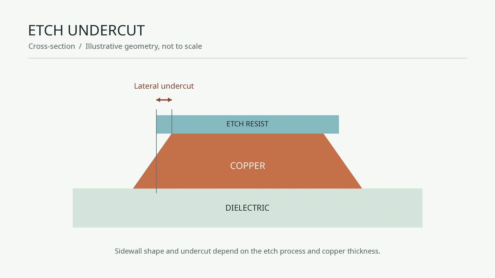
In subtractive processing, etchant removes unwanted foil and can also cut sideways under the resist. That undercut consumes a larger share of the feature as the line gets narrower; copper thickness and process control matter too.
Semi-additive processes generally plate copper into openings in resist over a thin conductive starting layer; a flash etch subsequently removes exposed starting copper. An mSAP route may use thin copper foil, while an SAP route may deposit a seed on the dielectric. Implementations vary, and the finished sidewall and minimum feature depend on the specific process.
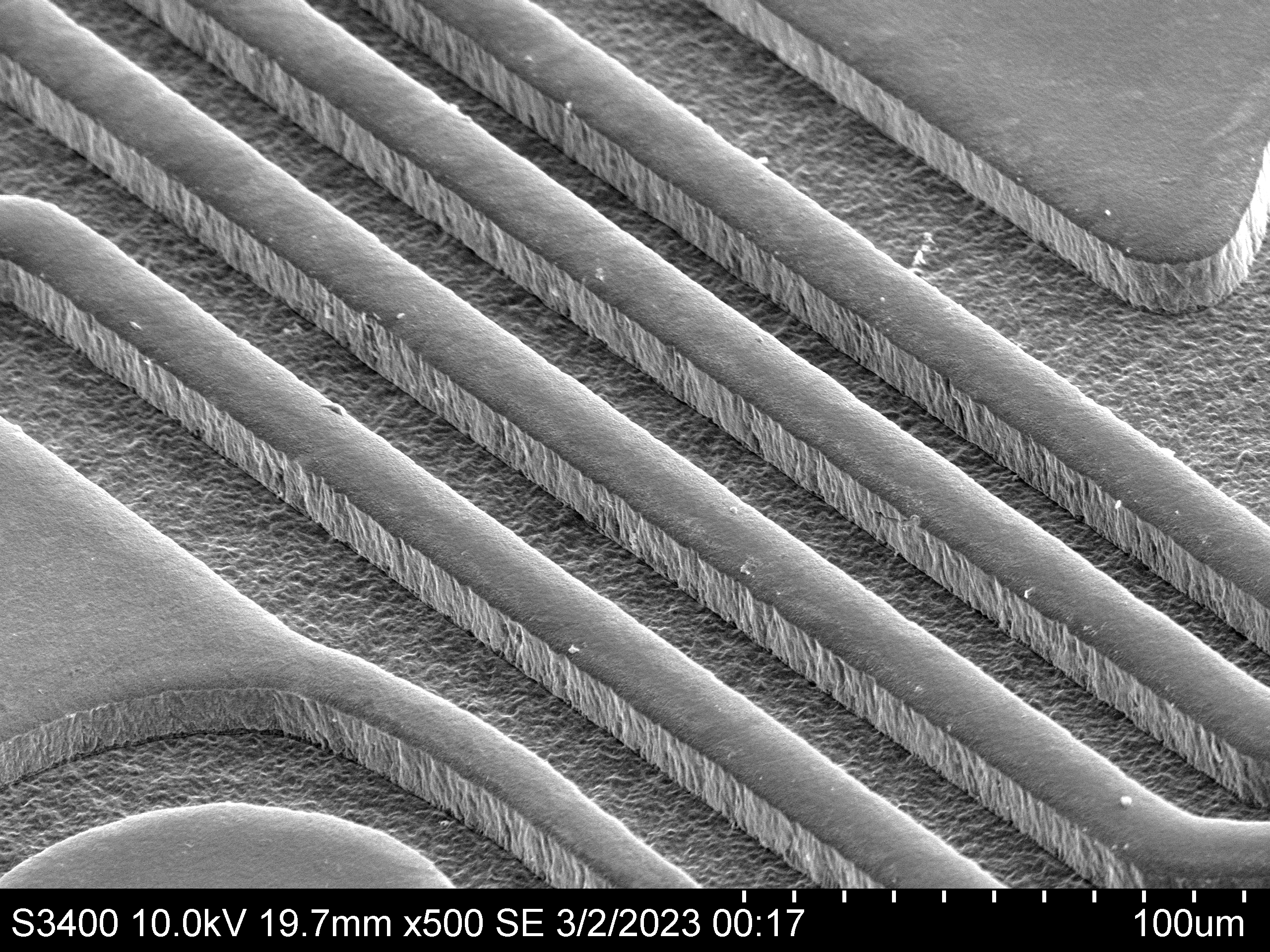
Plated copper features on an IC substrate at 500× magnification. This image is not identified as a specific SAP or mSAP build.
The question for a designer is not which process sounds more advanced, but which line and space the design actually needs, on which layers, and what that changes in resistance, impedance, cost and supplier choice.
1. How Each Process Forms a Trace
| Step | Subtractive (print and etch) | mSAP | SAP |
|---|---|---|---|
| Starting copper | Copper foil | Thin copper foil in a common implementation | Conductive seed deposited on dielectric in a common implementation |
| Imaging | Resist covers the traces | Resist covers the spaces | Resist covers the spaces |
| Copper build-up | Pattern or panel plating, then etch | Electroplate the traces to full thickness | Electroplate the traces to full thickness |
| Copper removal | Etch the full foil thickness between traces | Flash etch the thin foil | Flash etch the seed |
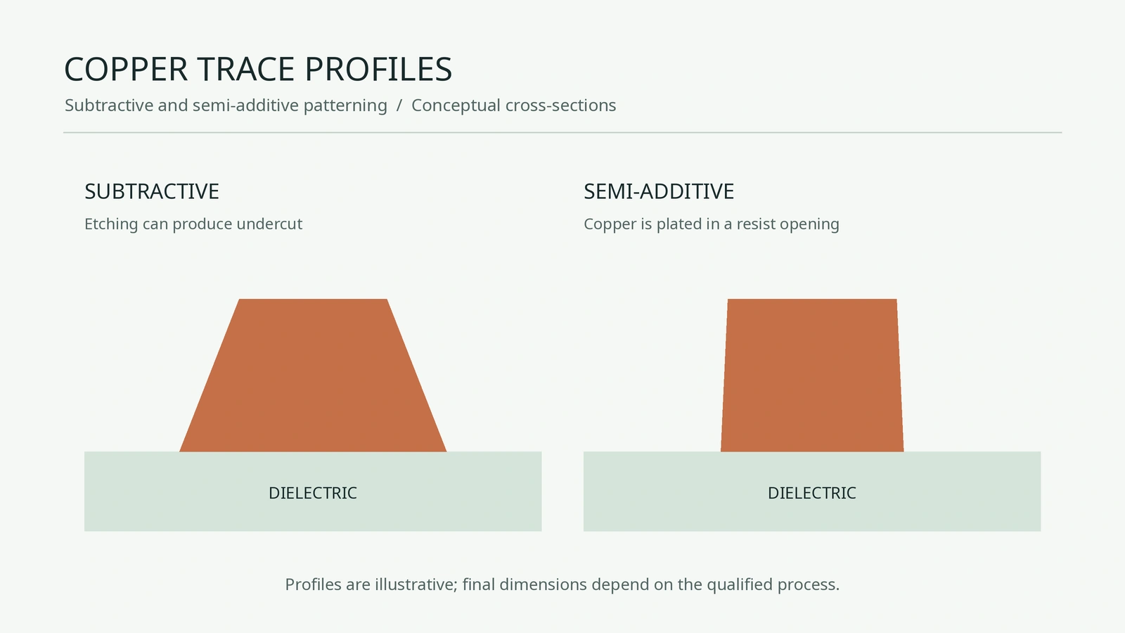
| Trace profile | Undercut can produce tapered sides | Plated profile, affected by processing | Plated profile, affected by processing |
| What affects line width | Imaging, etch and copper thickness | Imaging, plating and flash etch | Imaging, plating and flash etch |
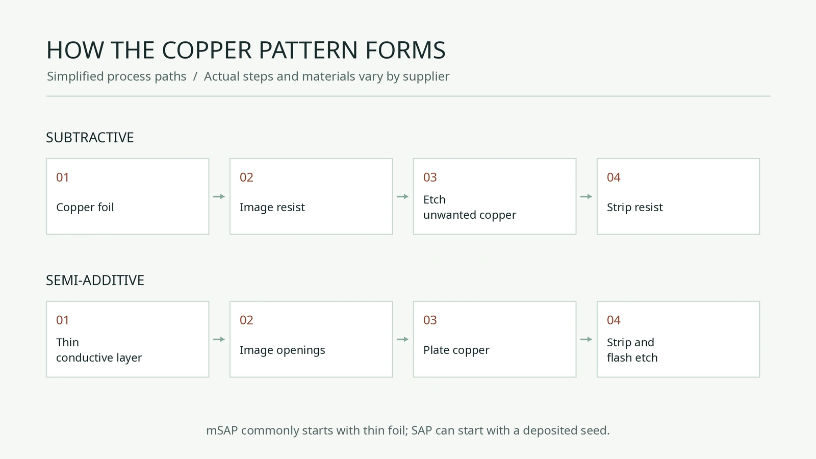
Imaging resolution, registration, plating and flash etching all affect finished geometry. Ask the fabricator how artwork compensation and inspection are applied; see also our LDI guide.
2. Comparison for Design Decisions
| Attribute | Subtractive | mSAP | SAP |
|---|---|---|---|
| Minimum line/space | Depends on qualified foil, imaging and etch | Depends on the qualified construction | Depends on the qualified construction |
| Finished trace thickness | Set by starting foil and any plating | Set by starting copper and plating | Set by seed and plating |
| Sidewall and width control | Etch undercut affects the finished profile | Resist, plating and flash etch affect the profile | Resist, plating and flash etch affect the profile |
| Dielectric | Laminates and prepregs selected for the build | Thin-foil laminates or build-up materials | Build-up materials selected for the build |
| Typical products | Most rigid, flex and HDI boards | Substrate-like PCBs, phone mainboards, ultra-HDI | IC package substrates, interposers |
| Supplier review | Confirm qualified geometry and stackup | Confirm fine-line layer and material options | Confirm substrate process and stackup options |
| Cost | Depends on construction and yield | Depends on construction and yield | Depends on construction and yield |
Values vary considerably between fabricators. Treat the table as a map of the territory, and use the qualified design rules of the supplier you will build with.
3. From BGA Pitch to Process: A Worked Decision
The usual reason a board needs fine lines is BGA breakout: how many traces must pass between two adjacent pads on a routing layer. With equal line and space, the gap between pads must hold n traces and n+1 spaces:
For pitch p, pad diameter d, and n traces, the ideal equal line and space is L = S = (p - d) / (2n + 1).
| BGA pitch | Pad diameter | Ideal gap | 1 trace: equal line/space | 2 traces: equal line/space |
|---|---|---|---|---|
| 0.50 mm | 0.25 mm | 250 µm | 83 µm | 50 µm |
| 0.40 mm | 0.22 mm | 180 µm | 60 µm | 36 µm |
| 0.35 mm | 0.20 mm | 150 µm | 50 µm | 30 µm |
| 0.30 mm | 0.18 mm | 120 µm | 40 µm | 24 µm |
These are ideal upper bounds with zero allowance for manufacturing tolerances, registration, solder mask, pad and via geometry or routing direction. For example, 36 µm at 0.4 mm pitch is a screening value, not a demonstrated breakout or a process requirement. Compare a layout with adequate margin against each supplier's qualified finished rules, and evaluate the layer and microvia alternatives with the fabricator. For BGA fan-out and via-in-pad, see our microvia guide.
4. Design Consequences of Thin, Narrow Copper
Resistance. The following DC estimates use R = ρ × length / (width × thickness), a 10 mm uniform rectangular copper section and assumed resistivity of 1.72 × 10⁻⁸ Ω·m. They exclude temperature changes, geometry tolerances, nonrectangular profiles, contacts, vias and AC effects.
| Trace (width × thickness) | Resistance per 10 mm |
|---|---|
| 75 × 18 µm (subtractive, ½ oz) | 0.13 Ω |
| 50 × 15 µm | 0.23 Ω |
| 30 × 12 µm (mSAP) | 0.48 Ω |
| 20 × 10 µm | 0.86 Ω |
| 15 × 8 µm (SAP) | 1.43 Ω |
Check voltage drop, heating and signal integrity against the actual circuit and finished geometry. Wider copper or a suitable plane may be needed where the current budget demands it.
Layer assignment. Identify the dense routing and power layers in the stackup. Different feature widths may coexist on a layer, but whether a mixed construction or process is available depends on the fabricator; confirm the proposed layer sequence and requirements.
Impedance. Sidewall shape, finished width, copper thickness and dielectric geometry affect impedance. Recalculate using the fabricator's finished stackup and ask which coupons and test tolerances are available.
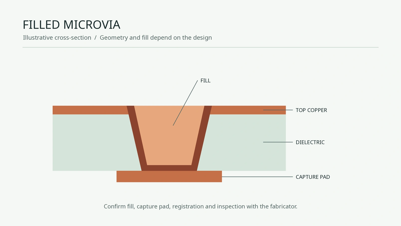
Microvias and registration. Fine-line layers usually sit on build-up dielectrics with laser microvias. Capture pads shrink with line width, so registration between the laser drill and the imaged layer is part of the budget; see our annular ring guide.
5. Cost and Lead-Time Drivers
| Driver | Why it matters |
|---|---|
| Number of fine-line layers | Affects process steps and stackup choices; compare supplier quotes |
| Minimum line/space | Each step down narrows the supplier base and the process window |
| Build-up count and microvia stacking | Sequential lamination cycles add time and yield risk |
| Material | Availability and qualification depend on the selected construction |
| Yield at the design's tightest feature | Feature distribution and process margins can affect yield |
| Test and inspection | Agree on AOI, coupons and cross-sections where applicable |
Using minimum geometry only in breakout regions, and opening up line and space elsewhere, is often the most effective cost lever.
6. RFQ and Stackup Checklist
- Mark the fine-line layers in the stackup and state the process expected (subtractive, mSAP or SAP), or ask the fabricator to propose it.
- Give minimum line and space per layer, and where on the layer it is needed (breakout region only, or full layer).
- State finished copper thickness required on fine-line layers.
- List controlled-impedance lines on fine-line layers with targets and tolerance.
- Define microvia structure: stacked or staggered, filled, capture pad sizes.
- Ask for qualified design rules from the fabricator before layout freeze.
HILPCB's IC substrate PCB page lists 25/25 µm standard and 15/15 µm advanced line/space, and 5–35 µm copper for advanced SAP builds. It separately states ±10% seed-layer uniformity and ±10% differential-etch width control. The HDI PCB page lists 75/75 µm standard and 50/50 µm advanced line/space. These individual listings do not establish that all parameters can be combined in one build. Send your stackup, BGA pitch, finished copper and layer requirements with a quote request for construction-specific confirmation.
FAQ
What is the difference between SAP and mSAP?
Both generally plate copper into a resist pattern and then remove exposed starting copper. A common mSAP route uses thin foil; a common SAP route deposits a conductive seed on the dielectric. Actual materials, geometry and process steps vary by supplier.
When does a PCB need mSAP?
Consider mSAP when the required finished geometry and stackup fall within a supplier's qualified mSAP construction. At 0.4 mm pitch and 0.22 mm pads, 36 µm is the ideal zero-margin equal-line/space value for two traces, not proof that a design fits or requires mSAP.
What line and space can subtractive etching achieve?
Limits vary with copper thickness, materials, tolerances and the supplier's qualified process. AT&S's miniaturization comparison includes a subtractive 40/40 µm example; that example is not a universal capability or a guarantee for another build.
Can I mix mSAP and conventional layers on one board?
Some stackups combine different layer constructions. Ask the fabricator whether the proposed combination and feature geometries are qualified for your order.
Do mSAP traces have higher resistance?
Resistance depends on the finished copper cross-section and conditions, not the process name alone. Under the stated rectangular DC model, a 30 × 12 µm trace is about 0.48 Ω per 10 mm, versus about 0.13 Ω for a 75 × 18 µm trace.