
Laser direct imaging (LDI) exposes photoresist or solder mask from digital CAM data instead of a film phototool. Imaging equipment can use optical targets on the panel to align the pattern and, depending on the machine and process, compensate for measured panel scale changes. The correction and remaining error depend on the targets, equipment, material movement and inspection method.
LDI can help with fine-pitch solder mask and fine-line copper imaging, but it does not fix every error called "registration." It cannot move inner-layer copper that has already shifted during lamination or correct drill wander. Ask for finished-feature requirements and measured alignment, not just an imaging method.
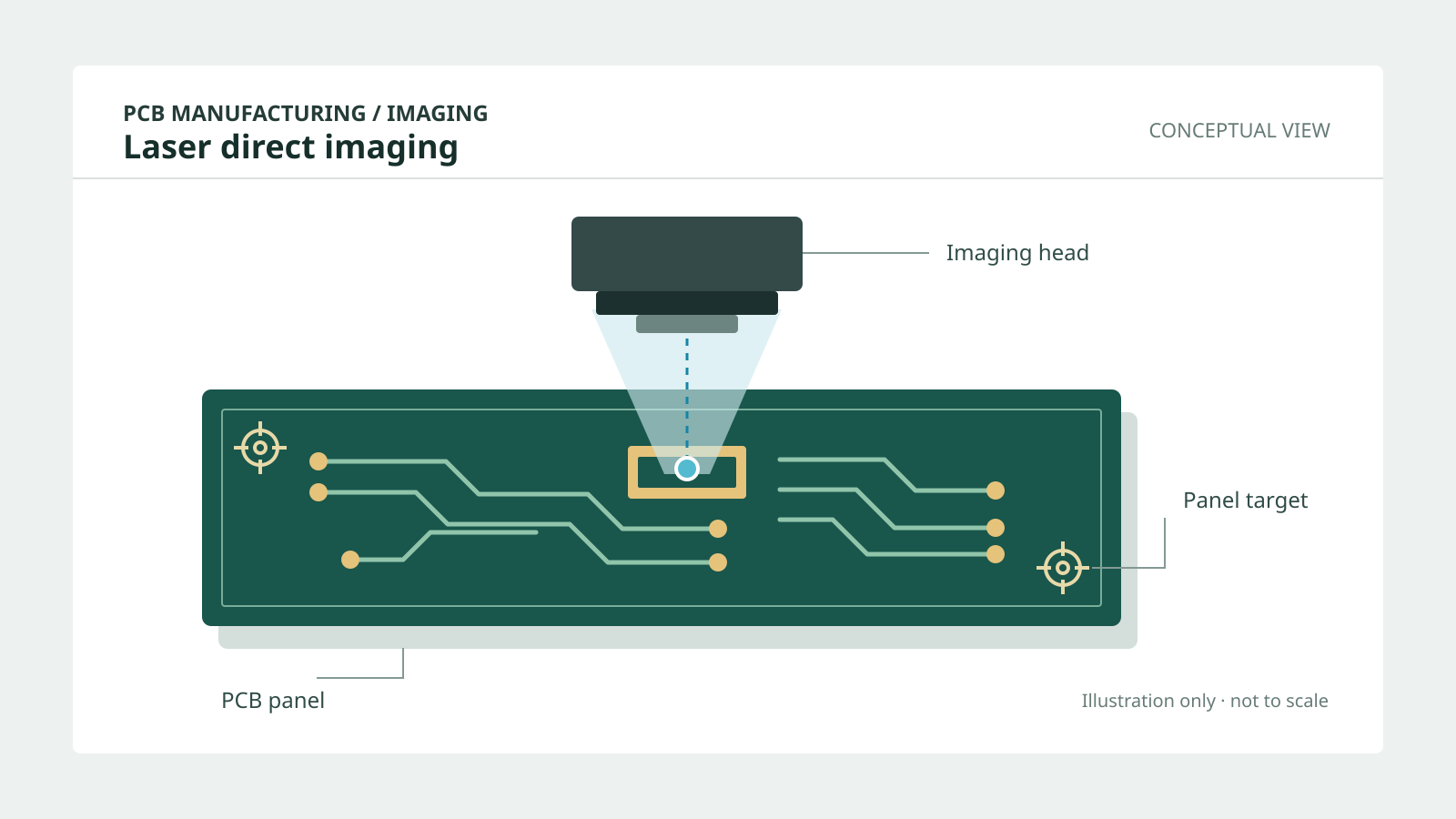
1. How LDI Places the Image
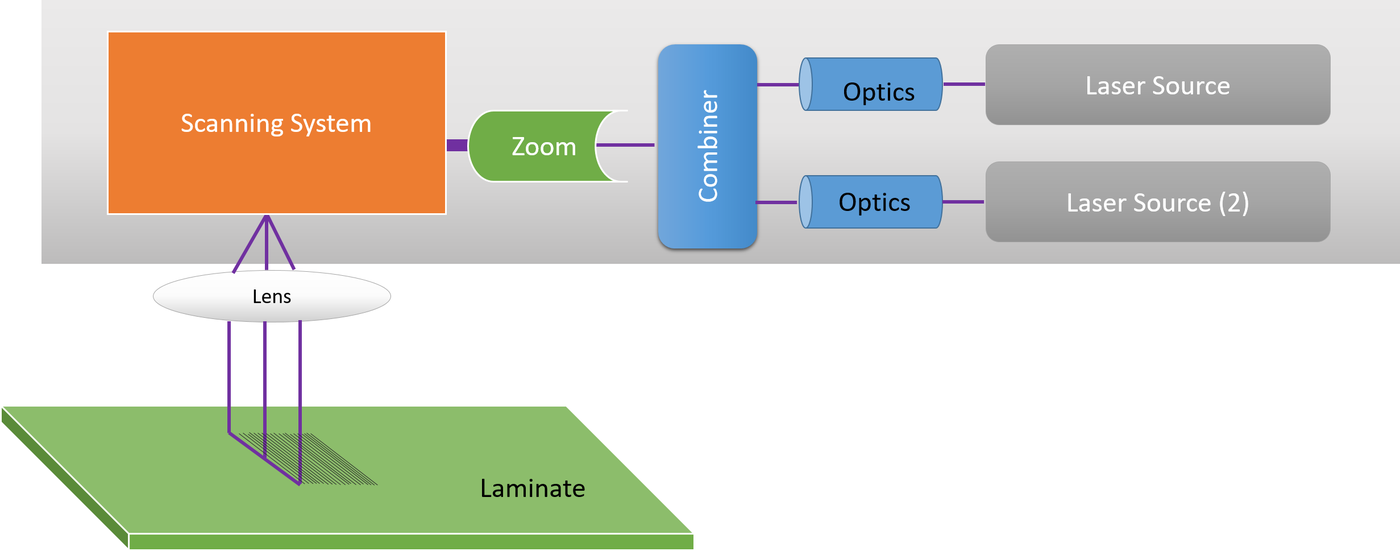
The following schematic shows one example of a laser scanning and optical arrangement; actual equipment configurations vary.
| Step | Film (contact) exposure | LDI |
|---|---|---|
| Image source | Phototool plotted from CAM data, then handled and stored | CAM data sent directly to the imager |
| Alignment | Film pinned or optically aligned to tooling | Optical targets align the image, subject to equipment and process |
| Scale correction | Compensation is set when the film is made | Some systems adjust image scale using measured panel targets |
| Film defects (dust, scratches, humidity-related changes) | Possible | Film-related defects do not apply |
| Job changeover | New film set | Load new data |
| Throughput | Depends on equipment and setup | Depends on the imager, material, exposure energy and job |
After exposure, the resist is developed and copper is etched or plated according to the fabrication route; solder mask is developed and cured according to its process.
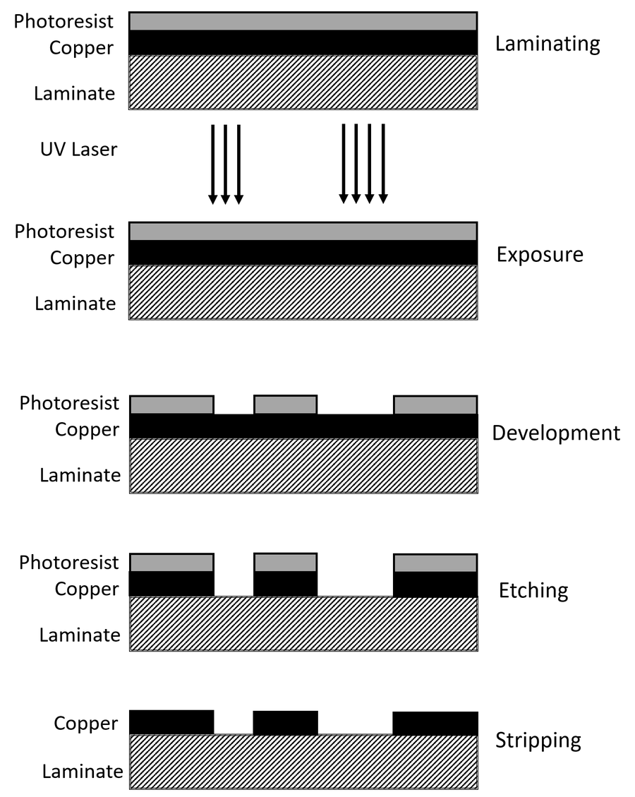
The sequence above illustrates a subtractive copper process; other resist types and plating routes can use different steps.
2. The Error Budget: What LDI Can and Cannot Correct
| Error source | Typical cause | LDI's role | Other controls |
|---|---|---|---|
| Film dimensional change | Temperature and humidity change the film | Film-related error is removed because no film is used | Control other imaging and material errors |
| Panel scale change | Material movement, glass style, resin flow | May compensate measured global scaling for the image being exposed | Stackup balance, material choice and process control |
| Image-to-hole alignment | Target, imaging and panel tolerances | Can align to suitable drilled targets; residual error remains | Verify image-to-hole registration on the finished process |
| Nonlinear local distortion | Uneven copper, local stress | Correction varies by machine; global scaling alone cannot remove local distortion | Balanced copper, process control and measured acceptance |
| Inner-layer core-to-core shift | Core registration during lamination | Cannot move copper already fixed in the laminate | Lamination tooling and suitable drill targeting |
| Drill position and wander | Spindle accuracy, deflection | Cannot correct the drilled hole | Drill process and appropriate drill-program compensation |
| Etch undercut and line-width variation | Etch chemistry, copper thickness | Imaging does not set the etch factor | Etch compensation and copper thickness control; see our etching precision guide |
| Mask opening size variation | Ink thickness, exposure, development | Imaging is only one part of the process | Mask process control; see our soldermask exposure guide |
Imaging registration describes image placement relative to a stated target. Layer-to-layer registration describes alignment between specified copper layers; drill-to-copper registration describes hole position relative to copper. Ask which layers, targets, measurement method and acceptance limits apply to each value. Annular ring calculations must account for the relevant hole-to-copper and finished-feature tolerances; see our annular ring design guide and registration tolerance guide.
3. Copper Layers: Fine Lines and Panel Scaling
Eliminating film avoids its handling defects and dimensional variation. Achievable features still depend on the imager, resist, exposure and downstream etching or plating; fine lines do not depend on LDI alone.
Consider a 500 mm span that grows by 100 ppm: it increases by 50 µm overall. If a fixed-scale image is ideally centered, the difference is about 25 µm at each end; if one end is fixed, it is about 50 µm at the other. These simplified cases exclude local distortion and other errors. A capable imager may compensate measured scale change, but final image-to-hole alignment must still be checked.
For very fine features, fabricators may combine direct imaging with subtractive, modified semi-additive or semi-additive processes, depending on the design and their capabilities. HDI and flex can benefit from careful target selection and scale compensation. For sequential lamination, ask which targets are used at each imaging step and how alignment to drilled features is verified.
4. Solder Mask: The Web Budget by Pitch
Opening expansion sets the nominal space between neighboring mask openings; mask-to-pad alignment determines how those openings sit over the copper. For equal pads and symmetric nominal expansion, the planned web is:
Here S_Cu is the copper gap and E is the nominal opening expansion per side. The following compares two hypothetical expansions, 60 µm and 35 µm, for the same pad geometry. They are illustrative design inputs, not film or LDI capability specifications or measured finished webs.
| Pitch | Land | Copper gap | Example A: expansion / nominal web | Example B: expansion / nominal web |
|---|---|---|---|---|
| 0.50 mm | 0.25 mm | 0.25 mm | 60 µm / 130 µm | 35 µm / 180 µm |
| 0.40 mm | 0.20 mm | 0.20 mm | 60 µm / 80 µm | 35 µm / 130 µm |
| 0.35 mm | 0.18 mm | 0.17 mm | 60 µm / 50 µm | 35 µm / 100 µm |
These widths are the space between nominal openings, not minimum finished mask. Registration shift affects mask coverage of pads, while opening-size variation, edge definition and development affect the remaining web. Ask the fabricator for its opening expansion, minimum finished web, measurement method and acceptance criteria. If individual webs cannot be reliably produced, discuss a gang opening and the package supplier's assembly requirements. Mask webs can help reduce bridging but do not guarantee its prevention. For layout rules, see our solder mask design guide.
5. When Film Exposure Is Still an Option
Film exposure can be appropriate when it meets the finished design requirements. Cost and throughput vary with equipment, material, setup, volume and revisions; compare actual quotations.
| Design condition | What to discuss with the fabricator |
|---|---|
| Component pitch | Whether individual webs are needed and can be inspected |
| Outer-layer line/space | Minimum finished dimensions and tolerances |
| Annular ring margin | Hole-to-copper registration and finished ring acceptance |
| Material | Movement, target selection and available compensation for the stackup |
| Volume and revisions | Setup, film, imaging time and revision costs |
| Mask color | Material compatibility and exposure route for the selected color |
Ask which route the fabricator proposes and whether it can meet the drawing. Naming a machine alone does not establish finished-feature acceptance.
6. Fabrication Notes and RFQ Checklist
- State the requirement where it matters: for example, specify the minimum finished mask web and where it applies. Agree on the measurement and acceptance method rather than relying only on an equipment name.
- Give the critical geometry: smallest pitch, minimum outer-layer line/space, and any controlled-impedance outer lines.
- Separate the registration numbers: ask for mask-to-pad, layer-to-layer and drill-to-copper registration using defined targets and acceptance limits.
- Name the mask color and confirm the proposed process is compatible with it.
- For flex and sequential lamination, ask how each image is aligned to the relevant targets and how the residual error is checked.
HILPCB's product information describes LDI and related capabilities for halogen-free multilayer boards, high-speed boards, HDI boards and flex boards. Applicable registration, line-width and inspection limits depend on the design and manufacturing route. Include the finest pitch, line/space and required mask webs in a quote request, and ask which tolerances and imaging route can be accepted for the order.
FAQ
What is laser direct imaging in PCB manufacturing?
It exposes photoresist or solder mask with a scanning laser driven by CAM data instead of a film phototool. Equipment can align the image to panel targets and may compensate measured scale change, depending on the system and process.
Does LDI improve layer-to-layer registration?
It can improve placement of an image relative to selected targets, but cannot move inner-layer copper that shifted during lamination or correct drill wander. The residual alignment must be measured against the relevant layer-to-layer or drill-to-copper requirement.
When do I need LDI solder mask?
Ask about LDI when fine-pitch pads need individual mask webs or tight mask-to-pad alignment. Whether it is needed depends on the fabricator's actual process, the required finished web and the assembly requirements, not pitch alone.
Does LDI make finer traces possible?
It avoids film defects and can support fine resist features. The achievable finished line and space also depend on the imager, resist, copper thickness and etching or plating process; LDI alone does not set the limit.
Is LDI more expensive than film exposure?
It can change imaging, setup and film costs, but the result depends on the equipment, mask material, production volume and number of revisions. Compare quotations for the actual design and acceptance criteria.