
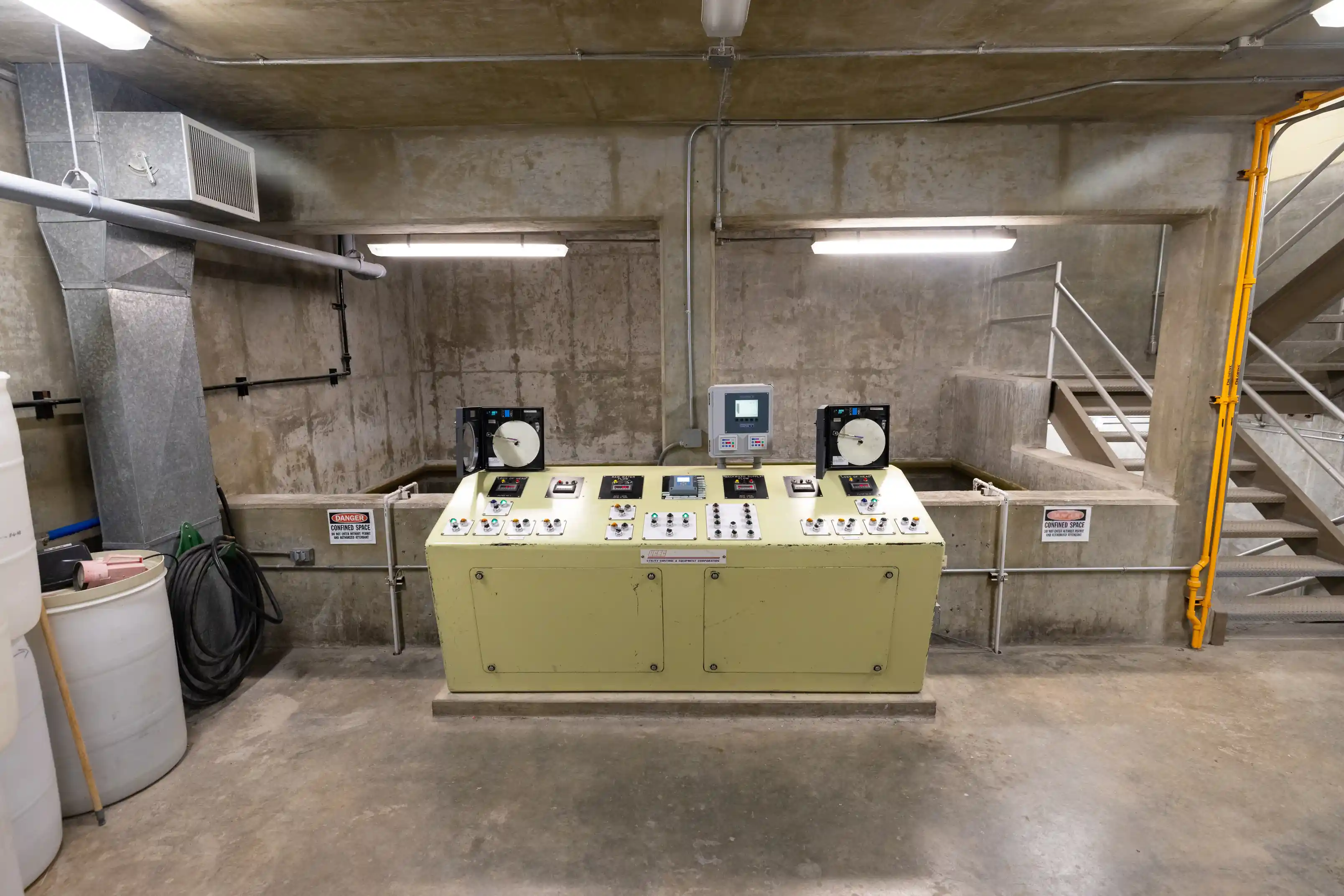
A nanofiltration PCB is the control and measurement board used inside a nanofiltration water-treatment system to read water-quality sensors, control pumps and valves, protect industrial communication ports, and keep process data stable in humid and electrically noisy environments. It does not make the membrane perform by itself; it supports the electronic control loop that helps the membrane skid operate within the pressure, flow, conductivity, pH, and safety limits defined by the system design.
Nanofiltration sits between ultrafiltration and reverse osmosis in many membrane-treatment architectures. The membrane process is usually selected for partial desalination, hardness reduction, color or organic-matter reduction, and selective removal of multivalent ions, while the electronics must keep the process measurable, controllable, and maintainable. For a PCB manufacturer, the real design burden is not the membrane chemistry. It is the board-level interface between wet process equipment and dry electronics.
Key Takeaways
- A nanofiltration PCB should be reviewed as a process-control and water-quality acquisition board, not as a generic environmental monitoring PCB.
- Conductivity, pressure, flow, pH, ORP, turbidity, temperature, and level interfaces create very different analog front-end requirements, so sensor channels should not be treated as interchangeable inputs.
- Pump motors, solenoid valves, VFDs, contactors, and long field cables create EMI, surge, and ground-loop risks that must be handled at the PCB port boundary.
- Humidity, condensation, chlorine-containing chemicals, acid/alkali cleaning fluids, and cabinet heat make conformal coating, connector selection, creepage planning, and cleaning process control central to reliability.
- A PCB can support ISO 15839-style online sensor performance testing, IEC 61000 EMC planning, or drinking-water monitoring programs, but final accuracy, regulatory acceptance, and water-quality compliance must be validated at the instrument or system level.
- The strongest RFQ package includes the process diagram, sensor list, pump and valve ratings, enclosure conditions, communication protocol, calibration method, expected cleaning chemicals, and test requirements.
In This Guide
- What a nanofiltration PCB actually controls
- Sensor interfaces for membrane monitoring
- Low-noise analog acquisition and calibration memory
- Pump, valve, and actuator control in wet industrial environments
- Moisture, corrosion, coating, and connector protection
- Industrial communication and remote monitoring
- Standards, validation, and compliance boundaries
- Common failure modes in water-treatment PCBs
- Cost drivers for nanofiltration control PCBs
- RFQ checklist for a nanofiltration PCB project
- Why work with HILPCB
- FAQ
- Next steps
What a nanofiltration PCB actually controls
A nanofiltration skid is not controlled from one measurement. The electronics usually have to watch several variables at the same time: feed pressure, concentrate pressure, permeate flow, concentrate flow, conductivity before and after the membrane, temperature, pH, valve state, pump current, leak detection, tank level, and alarm contacts. A well-designed PCB turns those signals into a stable control and diagnostic layer.
At board level, the design normally has four responsibility zones.
The first zone is measurement. The board receives low-level analog signals from probes or higher-level industrial signals from transmitters. Conductivity, pH, ORP, turbidity, pressure, flow, and temperature all behave differently, so the PCB must match the electrical interface to the sensor type instead of forcing every sensor through the same input circuit.
The second zone is control. The PCB may drive relays, opto-isolated outputs, MOSFETs, solenoid valves, pump-enable lines, dosing pumps, cleaning valves, or fan outputs. Even when a PLC or upper controller owns the main logic, the local PCB still needs robust I/O conditioning and protection.
The third zone is communication. Nanofiltration equipment often reports to a PLC, HMI, SCADA system, building-management system, or cloud gateway. That can involve RS-485/Modbus RTU, CAN, Ethernet, Wi-Fi, cellular, or a custom serial protocol. The communication circuit must survive field wiring errors and industrial transients without corrupting measurements.
The fourth zone is protection and serviceability. Water-treatment cabinets are humid, chemically active, and frequently serviced. The board must tolerate condensation risk, connector handling, cleaning-fluid vapor, cable surges, and repeated maintenance access. This is where coating, gold-finish contact areas, mechanical strain relief, spacing, and test points become reliability features rather than optional details.
| PCB responsibility | Typical signals or loads | Board-level design focus | What not to overclaim |
|---|---|---|---|
| Water-quality measurement | Conductivity, TDS estimate, pH, ORP, turbidity, temperature | Low leakage, low noise, stable reference, sensor excitation, calibration data | Do not claim final water compliance from PCB data alone |
| Hydraulic monitoring | Pressure, differential pressure, flow, level, leak detection | Protected analog inputs, pulse inputs, debounce, isolation where needed | Do not assume one sensor accuracy applies to every transmitter |
| Process control | Pumps, valves, dosing, flushing, CIP sequence support | High-current paths, flyback suppression, relay/MOSFET layout, safe default states | Do not imply PCB alone validates process chemistry |
| Communication | RS-485, Ethernet, CAN, wireless module, HMI link | Surge/ESD protection, isolation, connector pinout, EMC layout | Do not claim protocol certification unless device-level testing exists |
| Harsh-environment protection | Humidity, condensation, cleaning chemicals, cabinet heat | Coating, creepage, connector selection, conformal-coating keep-outs | Do not treat coating as a substitute for enclosure design |
The review should start from the process diagram. A PCB for a small point-of-use nanofiltration appliance, an industrial membrane skid, a wastewater polishing unit, and an online monitoring station can all use the phrase Nanofiltration PCB, but they do not ask for the same I/O count, isolation level, enclosure strategy, or validation plan.
Sensor interfaces for membrane monitoring
Sensor input design is the most important part of a nanofiltration PCB because the controller can only make good decisions from stable measurements. The board should document each sensor channel by signal type, supply voltage, isolation need, connector pinout, calibration method, and fault detection behavior.
Conductivity and TDS-related measurement is central to many membrane systems. Conductivity is often used to estimate dissolved ionic content and monitor rejection trend, but the PCB should not describe conductivity as a universal water-quality proof. A conductivity input may require an AC excitation source, low-noise current or voltage measurement, temperature compensation, and careful guard or shielding strategy to reduce leakage error. If the project uses a transmitter with a 4–20 mA or 0–10 V output, the PCB burden shifts from probe excitation to protected industrial input design.
pH and ORP inputs need special attention because glass electrodes are high-impedance sources. Leakage currents, flux residue, moisture, and connector contamination can create major errors. For direct-electrode designs, the analog front end should use very high input impedance, low input-bias current, clean guard routing, and strong separation from digital or switching circuits. Many industrial systems avoid this burden by using a local pH transmitter and sending a conditioned signal to the control PCB.
Pressure and differential-pressure measurement drives membrane protection. Feed pressure, concentrate pressure, and permeate pressure may be used to estimate transmembrane pressure and detect fouling or blockage trends. Many pressure sensors provide conditioned voltage or current outputs, but the PCB still needs surge protection, filtering, ADC range matching, and diagnostic handling for open-circuit or short-circuit faults.
Flow measurement may arrive as pulse, frequency, analog, or digital data. Pulse-output flow meters need clean edge detection, debounce or filtering, ESD protection, and attention to long-cable noise. Analog flow transmitters need protected ADC inputs and sometimes isolation from the noisy pump-drive domain.
Turbidity and optical sensors are more common in pretreatment, feed-water monitoring, and fouling diagnosis than inside the membrane module itself. If the PCB drives the LED and reads the photodiode directly, the board must manage LED current stability, optical detector noise, ambient-light rejection, and calibration storage. If the project uses a commercial turbidimeter with a digital or analog output, the PCB should focus on protected interface design.
| Parameter | Why it matters in nanofiltration | Common electrical interface | PCB design notes |
|---|---|---|---|
| Conductivity / resistivity | Tracks ionic content and rejection trend | Direct probe, 4–20 mA transmitter, 0–10 V, RS-485 | Use stable excitation or protected transmitter input; include temperature compensation path |
| pH / ORP | Supports membrane compatibility, dosing, CIP, and corrosion control | Direct high-impedance probe or transmitter output | Keep leakage low; guard sensitive nodes; isolate from switching and relay zones |
| Pressure / differential pressure | Protects membrane modules and supports fouling detection | 4–20 mA, 0–5 V, 0–10 V, digital | Protect against surge and wiring error; filter pump ripple without hiding real events |
| Flow | Confirms production rate, reject flow, flushing, and recovery ratio | Pulse, frequency, analog, digital | Provide clean edge detection and long-cable protection |
| Temperature | Supports compensation and equipment protection | RTD, NTC, digital, transmitter | Separate sensor accuracy from PCB measurement resolution |
| Turbidity / optical | Monitors pretreatment quality and suspended solids trend | Photodiode front end or analyzer output | Control LED drive stability and optical detector noise if measured directly |
| Level / leak detection | Prevents dry-run, overflow, or cabinet water damage | Float switch, conductivity leak sensor, capacitive sensor | Use fail-safe input logic and connector placement away from high-voltage areas |
A good release package should name whether the PCB is reading raw sensors or industrial transmitters. Raw sensors create analog-front-end, leakage, calibration, and noise challenges. Transmitters reduce analog burden but add field-wiring, surge, isolation, and protocol-integration requirements.
Low-noise analog acquisition and calibration memory
Water-treatment measurement is often slower than RF or high-speed digital design, but it is not simple. The signals can be small, high impedance, drift-prone, or exposed through long cables. A nanofiltration PCB therefore needs analog discipline: clean references, grounded shielding strategy, input protection, stable power, and careful layout around ADC inputs.
The analog acquisition chain normally follows a sequence:
- Sensor excitation or transmitter supply
- Input protection and filtering
- Signal conditioning or level shifting
- ADC conversion
- Temperature compensation
- Calibration correction
- Fault detection and data validation
- Storage or communication to the controller
This chain should be treated as one system. Adding a high-resolution ADC is not enough if the reference voltage is noisy, the ground path carries pump current, or the pH input is contaminated by flux residue. Similarly, strong filtering can hide electrical noise but also delay detection of real pressure spikes or flow changes if the time constant is chosen blindly.
| Acquisition issue | PCB-level cause | Design control |
|---|---|---|
| pH or ORP drift | Leakage across contaminated surfaces, high humidity, poor guarding | High-impedance layout, guard rings, clean process control, coating keep-out around sensitive nodes |
| Conductivity instability | Excitation noise, polarization, cable coupling, temperature variation | Stable AC excitation, shielding, temperature sensor pairing, calibration coefficients |
| Pressure reading ripple | Pump pulsation, VFD noise, ground bounce | Input filtering, differential measurement where appropriate, local decoupling, sensor ground planning |
| ADC code jump | Noisy reference, digital return current through analog ground | Separate analog region, star or controlled ground return, low-noise reference layout |
| False alarm | Long-cable surge, ESD, contact bounce | TVS/ESD protection, RC filtering, debounce logic, isolation as required |
| Calibration mismatch | Coefficients not tied to channel, sensor, or board revision | Nonvolatile memory, serial number tracking, production test data mapping |
For many designs, a 16-bit ADC is sufficient when the sensors are already conditioned by transmitters. A 24-bit ADC may be justified for high-resolution direct measurement, but only if the analog noise, reference stability, layout, and calibration method can support it. Resolution should be chosen from the measurement budget, not from a marketing target.
Calibration memory is also part of the PCB architecture. Boards used in water-quality systems may need to store channel gain and offset, temperature-compensation coefficients, sensor serial numbers, calibration date, fault logs, or firmware revision. This does not make the PCB a regulatory recorder by itself, but it does support a traceable instrument design when the system owner needs it.
Pump, valve, and actuator control in wet industrial environments
Nanofiltration systems rely on mechanical movement: high-pressure pumps, feed valves, concentrate valves, permeate valves, flush valves, chemical dosing pumps, and sometimes fans or cabinet heaters. These loads make the PCB electrically noisy and mechanically stressed.
Pump-control electronics should be separated from sensor acquisition. Motor starts can create voltage dips, ground bounce, inductive spikes, and broadband EMI. If the board places high-current motor paths near pH, conductivity, ADC, or reference circuits, measurement instability is predictable. A good layout creates clear zones for power input, actuator drive, sensor acquisition, communication, and logic control.
Valve outputs need proper flyback or transient suppression. A solenoid valve that looks small in the schematic can produce a voltage spike large enough to reset logic or damage an output transistor when switched repeatedly. Relay coils, MOSFET loads, and contactor-drive outputs all need suppression close to the source and return paths that do not inject noise into sensitive measurement ground.
For larger systems, the PCB may not drive the pump motor directly. Instead, it may send enable, analog speed command, digital control, or fault-interface signals to a VFD or pump controller. That shifts the PCB problem from high-current motor drive to industrial I/O protection, isolation, and noise immunity. The release package should make this distinction explicit.
| Control load | Typical PCB interface | Main risk | Layout recommendation |
|---|---|---|---|
| Solenoid valve | MOSFET, relay, low-side/high-side driver | Inductive kick, output overheating, cable surge | Place suppression near driver/connector; keep current loop compact |
| Dosing pump | Relay, isolated digital output, analog control | EMI, inaccurate dosing trigger, stuck output | Use isolated or protected I/O; include test points for output verification |
| High-pressure pump | Enable line, VFD command, contactor interface, sometimes motor driver | VFD noise, ground loops, power dips | Separate pump interface from sensor AFE; isolate long field cables where needed |
| Fan or cabinet heater | MOSFET/relay output | Thermal runaway, contact wear | Add thermal monitoring and current margin |
| Alarm beacon or buzzer | Digital output | Noise injection into logic rail | Decouple and separate return path from ADC reference |
Power design should follow the same zoning logic. The board may need one domain for field power, one for actuator outputs, one for digital logic, one for analog measurement, and one for communication isolation. A multilayer PCB stackup helps keep return paths controlled, while heavy copper PCB may be appropriate when the board carries sustained valve, relay, pump-interface, or heater current.
Moisture, corrosion, coating, and connector protection
Water-treatment cabinets are harsh electronic environments. Even if the PCB never touches liquid water, it may face condensation, high relative humidity, chlorine or oxidant vapor, acid/alkali cleaning chemicals, salt aerosols, and long service intervals. These conditions make protection design central to the board, not a final cosmetic step.
Conformal coating can reduce moisture and contamination risk, but it is not a universal fix. Acrylic, urethane, silicone, and parylene coatings behave differently in chemical resistance, repairability, dielectric strength, flexibility, and process cost. Coating also requires keep-outs around connectors, calibration contacts, test pads, switches, heat sinks, and some high-impedance sensor input areas. If the coating process is added after the PCB layout is frozen, it can create inspection and service problems.
Surface finish affects solderability, contact reliability, and corrosion resistance. ENIG is often used when fine-pitch components, long shelf life, or contact reliability matter, but the best surface finish depends on assembly process, connector design, cost, and chemical exposure. OSP can be cost-effective for many boards but is not automatically the right answer for exposed service conditions.
Connectors often fail before the PCB laminate fails. Field wiring terminals, M12 connectors, waterproof cable glands, board-to-wire headers, and pluggable terminal blocks should be selected with service environment, current, sealing, keying, vibration, and maintenance access in mind. A gold-plated contact or sealed connector may matter more than a more expensive laminate if the failure mode is cabinet condensation at the terminal zone.
Creepage and clearance should be reviewed with pollution degree, voltage, coating, and installation context in mind. A low-voltage sensor board in a sealed IP-rated module has a different requirement from a mixed-voltage controller sharing a cabinet with AC mains, pump contactors, and VFD wiring.
| Environmental threat | Board-level symptom | Design response |
|---|---|---|
| Condensation | Leakage, ADC drift, corrosion, false sensor input | Coating, spacing, drainage orientation, sealed connectors, humidity-aware enclosure design |
| Chemical vapor | Corroded contacts, tarnished finish, brittle coating | Chemical-compatible coating and connector selection; avoid exposed copper |
| Cleaning-fluid splash | Temporary short, residue buildup, connector failure | IP-rated enclosure strategy, coating keep-outs, gasket and cable entry planning |
| Vibration and maintenance handling | Cracked solder joints, loose terminal screws, broken wires | Mechanical support, strain relief, through-hole or reinforced connectors where needed |
| Cabinet heat | Electrolytic capacitor aging, regulator derating, coating stress | Thermal vias, copper spreading, component derating, airflow or conduction path review |
| Ionic contamination | Leakage around high-impedance inputs | Cleaning process control and ionic contamination review for sensitive designs |
A high-Tg PCB can help when cabinet temperature, assembly temperature, or dimensional stability are concerns, but Tg is only one part of environmental reliability. Coating, cleaning, connectors, enclosure design, and field-wiring practice are often just as important.
Industrial communication and remote monitoring
Nanofiltration systems rarely operate as isolated electronics. They normally communicate with an HMI, PLC, SCADA system, remote monitoring gateway, or cloud dashboard. The PCB should support communication without allowing long field cables and network ports to become the main failure path.
RS-485 remains common for Modbus RTU and other field communication because it is simple, robust, and cost-effective. A good RS-485 port needs ESD protection, common-mode management, bias/termination planning, and isolation where ground potential differences are expected. Termination should be documented clearly; it should not be left to installation guesswork.
Ethernet may be used for higher data volume, local web configuration, firmware update, or plant network integration. Ethernet ports should include magnetics, ESD protection, connector shielding strategy, and a clear boundary between chassis and signal ground. Industrial Ethernet is not only a protocol decision; it is a PCB layout and connector-zone decision.
Wireless modules are useful for remote skids, temporary monitoring, or distributed environmental stations, but the PCB must protect the RF design from the cabinet environment. Antenna placement, enclosure material, ground clearance, keep-out zones, and cable routing can matter more than the module part number. Cellular, Wi-Fi, LoRa, or NB-IoT integration also changes power budgeting because transmission bursts can disturb analog measurement if the supply is weak.
| Communication route | Where it fits | PCB design focus |
|---|---|---|
| RS-485 / Modbus RTU | Local plant wiring, PLC/SCADA link, multi-drop sensors | Isolation, surge/ESD, termination, biasing, shield strategy |
| CAN / CANopen | Distributed modules, pump or valve controllers | Differential routing, common-mode protection, connector pinout control |
| Ethernet | HMI, controller link, remote diagnostics, firmware update | Magnetics, ESD, controlled impedance, chassis/shield handling |
| 4–20 mA / dry contact | Simple industrial integration, alarm and status output | Input/output protection, isolation, terminal labeling |
| LoRa / NB-IoT / LTE | Remote or distributed sites | Antenna keep-out, burst current, RF ground, enclosure effect |
| USB / service UART | Commissioning and maintenance | ESD protection, access without opening unsafe areas, clear service procedure |
The PCB supports a communication and monitoring architecture. Do not describe the device as SCADA-ready, cybersecurity-compliant, or regulator-approved unless the full instrument has been tested and documented in that environment.
Standards, validation, and compliance boundaries
Water-treatment and environmental-monitoring products often sit near standards and regulations, but the PCB is only one part of the final instrument. The board can support accurate sensing, data integrity, EMC test planning, calibration storage, and traceable production. It cannot by itself prove drinking-water compliance, wastewater discharge compliance, sensor accuracy, or cybersecurity acceptance.
A practical boundary is:
- PCB-level control: layout, protection, isolation, ADC design, power integrity, cleaning, coating, manufacturing test, traceability.
- Instrument-level control: sensor calibration, enclosure sealing, probe installation, firmware algorithms, data logging, user interface, communication protocol, EMC testing.
- System-level control: membrane performance, sampling location, water chemistry, maintenance schedule, regulatory reporting, plant operating procedure.
ISO 15839 is relevant because it covers performance testing of online sensors and analyzing equipment for water. A PCB can support that style of instrument validation by providing stable acquisition, calibration memory, and diagnostic data, but the standard applies to the sensor or analyzer equipment rather than to the bare PCB alone.
IEC 61000-series EMC standards are also system-level context. A PCB can improve ESD, EFT, surge, and radiated/conducted noise behavior through protection parts, grounding, shielding, and layout. The pass/fail result belongs to the equipment configuration, enclosure, cable setup, firmware state, and test plan.
Drinking-water or wastewater regulations should be handled even more carefully. A water-quality PCB can measure and log parameters, but the legal compliance of treated water depends on sampling method, approved test method, calibration, water chemistry, process operation, and jurisdiction-specific rules. Do not write that a PCB makes water compliant.
Reference standards and guidance to consider
- ISO 15839 — Water quality, online sensors/analyzing equipment, specifications and performance tests
- IEC 61000-4-2 — Electrostatic discharge immunity test
- IEC 61000-4-4 — Electrical fast transient/burst immunity test
- IEC 61000-4-5 — Surge immunity test
- IEC 61000-6-2 — Immunity for industrial environments
- IEC 61000-6-4 — Emission standard for industrial environments
- IEC 60529 — Degrees of protection provided by enclosures, IP code
- IPC-A-610 — Acceptability of electronic assemblies
- IPC-6012 — Qualification and performance specification for rigid printed boards
- RoHS Directive — Restriction of hazardous substances for applicable markets
- EU Drinking Water Directive — System-level drinking-water context for applicable products
- U.S. EPA water monitoring guidance — Monitoring-parameter and calibration context for applicable programs
These references should be used to plan design and validation. They should not be turned into PCB-only compliance claims.
Common failure modes in water-treatment PCBs
The most expensive failures in nanofiltration electronics often look ordinary at first: drifting measurements, random resets, intermittent communication, or a valve output that fails after months of service. The root cause is usually an interface or environment issue that was not visible in the schematic alone.
| Failure mode | Likely PCB cause | System symptom | Prevention during design review |
|---|---|---|---|
| Conductivity reading drifts upward or downward | Leakage, poor excitation stability, contamination near probe input | False rejection trend, unnecessary cleaning alarm | Guard sensitive nodes, clean AFE area, store calibration data, review coating keep-outs |
| pH channel becomes unstable in humidity | High-impedance node exposed to residue or condensation | Erratic pH control, dosing error | Use high-impedance layout rules, keep flux away, isolate connector area, specify cleaning |
| Controller resets when pump starts | Shared supply path, insufficient bulk capacitance, EMI from motor interface | Random shutdown, lost data, false alarm | Separate power domains, add input filtering, review ground return and surge path |
| RS-485 communication drops intermittently | Poor termination, missing isolation, cable surge, ground potential difference | SCADA timeout, missing data | Define termination/biasing, isolate field port when required, add ESD/surge protection |
| Valve output transistor fails | No flyback suppression, undersized MOSFET, poor thermal path | Valve stuck open/closed, no flushing or dosing | Add suppression, derate driver, use thermal copper and test points |
| Corrosion at terminal area | Unsealed connector, unsuitable plating, chemical vapor | Intermittent sensor or actuator failure | Select sealed or plated connectors; review enclosure and coating strategy |
| ADC noise increases after assembly | Poor cleaning, analog/digital return coupling, noisy reference | Reduced measurement repeatability | Control cleaning process, separate analog region, protect reference and ADC layout |
| Coating blocks service or calibration | No keep-out planning | Test pads unusable, connector service issue | Define coating drawing before production and include masked areas |
A good DFM review should therefore include more than trace width, hole size, and solder mask. It should review analog leakage risk, port protection placement, coating keep-outs, connector orientation, creepage/clearance assumptions, service access, and whether the first build can be tested realistically.
Cost drivers for nanofiltration control PCBs
Nanofiltration PCB cost is driven less by the keyword and more by the interface mix. A simple board that reads transmitter outputs and sends Modbus data is very different from a mixed-signal controller with direct pH input, conductivity excitation, valve drivers, isolated RS-485, Ethernet, cellular, coating, and functional calibration.
| Cost driver | Why it increases cost | How to control it |
|---|---|---|
| Number of sensor channels | More ADC inputs, connectors, calibration steps, and protection parts | Group channels by signal type and remove unused universal inputs |
| Direct sensor measurement | Requires low-leakage AFE, excitation, high-resolution ADC, calibration | Use transmitters when accuracy ownership is better kept outside the PCB |
| Isolation | Adds isolators, isolated DC-DC modules, creepage spacing, board area | Isolate only the field interfaces that need it |
| Actuator current | Requires copper width, thermal design, drivers, suppression | Separate high-current loads from measurement board when practical |
| Communication options | Ethernet, RS-485, wireless, and cellular add parts and testing | Define one primary interface and one service interface when possible |
| Environmental protection | Coating, sealed connectors, ENIG, high-Tg material, cleaning control | Match protection to actual enclosure and chemical exposure |
| Functional testing | Calibration, sensor simulation, output load testing, communication test | Provide test pads, programming headers, and automated test commands |
| Certification support | EMC pre-scan, documentation, traceability, material declarations | Define target markets and standards before layout release |
The cheapest board is not always the lowest-cost system. In water treatment, a few dollars saved on protection or connector quality can create service calls that cost far more than the PCB itself. The goal is not to overbuild every design; it is to match protection, isolation, and test depth to the real site exposure.
RFQ checklist for a nanofiltration PCB project
To quote and review a nanofiltration control PCB accurately, send more than Gerber files. The most useful RFQ package explains the process, sensor interfaces, environment, and testing expectations.
1. Design files
- Gerber, ODB++, or IPC-2581 files
- Drill files and stackup requirement
- Schematic, if DFM/DFT review is requested
- BOM with manufacturer part numbers and approved alternates
- Assembly drawing, polarity notes, and connector orientation
- Coating drawing with keep-outs and masked areas
- Firmware programming and test instructions, if PCBA is required
2. Sensor and I/O information
- Sensor list: conductivity, pH, ORP, pressure, flow, temperature, turbidity, level, leak detection
- Signal type for each channel: direct probe, 4–20 mA, 0–10 V, pulse, RS-485, I²C, SPI, UART
- Required measurement range, resolution, and calibration method
- Cable length and shielding requirement
- Actuator list: pumps, valves, relays, dosing, fan, alarm output
- Maximum load current and switching frequency
3. Environment and enclosure
- Indoor cabinet, outdoor enclosure, or exposed skid location
- Temperature and humidity range
- Condensation risk
- Chemical exposure: chlorine, acid, alkali, CIP chemicals, salt mist, disinfectants
- Enclosure IP rating target, if known
- Vibration or service-handling conditions
4. Power and communication
- Input power range: DC, AC, battery-backed, or redundant supply
- Isolation requirement between field, logic, analog, and communication zones
- Communication protocol: Modbus RTU, Ethernet, CAN, wireless, custom protocol
- Connector type and pinout
- Surge, ESD, EFT, or EMC test targets, if defined
5. Manufacturing and validation
- Prototype quantity and production forecast
- IPC class expectation
- Surface finish preference
- Conformal coating or potting requirement
- Functional test plan or sensor-simulation requirement
- Calibration data handling
- Traceability, labeling, serialization, and packaging needs
A complete RFQ lets the PCB team review the real risk areas early: analog leakage, port protection, actuator current, coating process, connector durability, and production test coverage.
Why work with HILPCB
HILPCB supports water-treatment and environmental-monitoring electronics from bare PCB fabrication through assembled board delivery. For nanofiltration projects, the value is strongest when manufacturing review starts before the board is locked.
Relevant capabilities include:
- Multilayer PCB stackups for controlled analog, digital, power, and communication domains
- High-Tg PCB options for higher cabinet-temperature and assembly-stability requirements
- Heavy copper PCB for higher-current valve, relay, power, or thermal paths
- Turnkey assembly for component sourcing, SMT/THT assembly, programming support, and functional test planning
- DFM and DFT review for connector placement, coating keep-outs, test access, and field I/O protection
- Process support for ENIG, solder-mask control, conformal-coating coordination, and production traceability
The goal is not to label the board as “compliant” before the system has been tested. The goal is to make the board easier to validate by reducing preventable causes of sensor drift, communication failure, corrosion, output-driver damage, and production-test ambiguity.
FAQ
What is a nanofiltration PCB?
A nanofiltration PCB is a control and monitoring board used in a nanofiltration water-treatment system. It reads sensors such as conductivity, pressure, flow, pH, ORP, turbidity, and temperature, then supports pump, valve, alarm, HMI, and communication functions.
Is a nanofiltration PCB the same as the nanofiltration membrane?
No. The membrane performs the physical separation process. The PCB supports measurement, control, communication, protection, and diagnostics around the membrane system. Membrane performance still depends on membrane chemistry, water chemistry, pressure, flow, pretreatment, cleaning, and system operation.
Which sensor interface is the most difficult on a water-treatment PCB?
Direct pH or ORP measurement is often one of the most sensitive because the electrode output is high impedance and vulnerable to leakage, contamination, and moisture. Conductivity measurement can also be challenging when the PCB must generate stable excitation and perform accurate temperature compensation.
Should the PCB read raw sensors or use industrial transmitters?
Use raw sensors when size, cost, or integration requires it and the design team can own calibration and analog performance. Use transmitters when the sensor manufacturer or system integrator should own probe excitation, compensation, and calibration, while the PCB reads protected 4–20 mA, 0–10 V, RS-485, or other conditioned signals.
Why does pump control create problems for sensor accuracy?
Pump motors, solenoid valves, contactors, and VFDs can generate voltage dips, transients, ground bounce, and EMI. If the PCB does not separate actuator current paths from analog measurement paths, sensor readings may drift, jump, or trigger false alarms.
Can conformal coating solve humidity problems by itself?
No. Conformal coating helps, but it must be combined with enclosure design, connector protection, cleaning control, spacing, coating keep-outs, and correct material selection. Coating can also create service and calibration problems if the layout does not plan masked areas.
Can the PCB prove drinking-water or wastewater compliance?
No. A PCB can support measurement, logging, and control, but water-quality compliance depends on the complete instrument, sensor calibration, approved sampling method, process operation, and jurisdiction-specific requirements. Final compliance must be verified at system level.
What files should I send for a nanofiltration PCB quote?
Send Gerber or ODB++ files, BOM, schematic if review is needed, sensor list, signal types, pump and valve ratings, cable lengths, communication protocol, power input, environmental conditions, coating requirement, and functional test expectations.
Next steps
If your nanofiltration controller is still facing sensor drift, pump-start resets, condensation risk, RS-485 communication drops, or uncertainty around coating and connector protection, do not wait until the first production run to resolve those issues.
Send the Gerber or ODB++ package, BOM, process I/O list, sensor interface table, power input range, and environmental requirements to [email protected], or upload the data through the Quote page. HILPCB can review the board for analog acquisition risk, field I/O protection, actuator current paths, coating keep-outs, connector durability, and manufacturability before you commit to the next build.