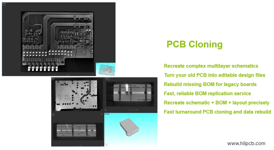
What is PCB cloning, and how does it actually work?
You've probably heard the term but don't understand the technical process. PCB cloning is the methodology for creating identical circuit boards from existing samples using specialized equipment and reverse-engineering techniques. This guide explains the actual technology, tools, and methods professionals use - not marketing fluff, but real technical processes.
Whether you're an engineering student, maintenance technician, or company evaluating cloning services, understanding the actual methodology helps you make informed decisions about when cloning is appropriate and what's realistically achievable.
The Technology Behind PCB Cloning
PCB cloning isn't magic - it's systematic application of inspection technology, component analysis, and manufacturing knowledge. Here's what actually happens:
1. Non-Destructive Board Imaging
Modern cloning starts with high-resolution digital imaging capturing every detail:
Optical Microscopy: Industrial cameras with 20-100x magnification photograph both board sides. Resolution: 10-50 microns per pixel capturing component markings, solder joints, and trace routing visible from surface. Specialized lighting (coaxial, ring light, darkfield) reveals different features.
X-Ray Computed Tomography (CT): For multilayer boards, industrial CT scanners create 3D volumetric data revealing internal structure. Technology similar to medical CT but higher resolution (5-10 micron voxels). Shows: internal layer routing, via connections, buried/blind via structures, BGA ball connections, and component internal construction.
Automated Optical Inspection (AOI) Systems: Originally designed for manufacturing quality control, AOI systems adapted for cloning work. Scan entire board automatically, generate measurement data, identify component packages, and create dimensional drawings through our PCB inspection technology.
2. Component Identification Technology
Determining what components populate the board requires multiple analysis techniques:
Visual Part Number Reading: Most components have manufacturer markings: full part numbers (easiest case), abbreviated codes requiring cross-reference, date codes and lot numbers, country of origin marks. Optical character recognition (OCR) software automates initial identification, but human verification essential due to similar-looking codes.
Package Analysis: When markings unclear or absent, package type identification narrows possibilities: package dimensions (length, width, height, pitch), pin count and arrangement, thermal pad presence, and body materials. Online package databases contain thousands of standard footprints aiding identification.
Electrical Characterization: For completely unmarked components, electrical testing determines function: semiconductor curve tracer reveals diode, transistor, or IC characteristics; LCR meter measures passive component values; function generator plus oscilloscope tests active components; pinout determination through systematic connectivity testing.
Destructive Analysis (Last Resort): When other methods fail: decapsulate IC packages chemically exposing die, photograph die and identify manufacturer from fabrication marks, use die database matching to determine chip function. Expensive and time-consuming, used only for critical unknown components.
3. Circuit Connectivity Mapping
Understanding how components connect requires systematic tracing:
Surface Trace Following: For 1-2 layer boards, trace all copper connections visible from top and bottom surfaces. Software tools: CAD import from scanned images, automated trace recognition algorithms, manual verification and correction.
Continuity Testing: Ohmmeter-based testing identifies nets: probe every component pin systematically, record which pins connect to which (resistance <1 ohm), build netlist documenting all connections. Tedious but necessary for multilayer boards where internal connections invisible.
X-Ray Layer Separation: CT scan data processed to separate individual copper layers: image processing algorithms identify copper versus dielectric, layers separated based on Z-axis position, trace routing reconstructed for internal layers, via connections mapped between layers.
4. PCB Stackup Determination
Multilayer boards require understanding internal construction through our PCB engineering analysis:
Cross-Sectioning: Cut board sample perpendicular to surface, polish cut surface to mirror finish, photograph under microscope measuring layer thickness, copper weight, dielectric material, and via structure. Provides definitive stackup information but destroys sample (requires spare board).
Non-Destructive Methods: Terahertz imaging penetrates PCB materials revealing layer structure without cutting, acoustic microscopy detects layer boundaries through ultrasound, capacitance measurement between layers estimates dielectric thickness. Less precise than sectioning but preserves board.
PCB Cloning Techniques by Board Complexity
Different board types require different approaches:
Simple Single-Sided Boards:
Technology Required: Basic digital camera, continuity tester, calipers for measurements. Process: Photograph top side, trace copper pattern in CAD software, measure board outline and hole positions, generate Gerber files for manufacturing. Timeline: Experienced technician completes in 2-4 hours. Success Rate: 99%+ for boards with standard through-hole components.
Double-Sided Boards:
Technology Required: High-resolution camera, X-ray machine (helpful but optional), continuity tester. Process: Photograph both sides separately, identify via locations connecting layers, trace top and bottom copper patterns, correlate connections between sides, verify with continuity testing. Timeline: 4-8 hours depending on complexity. Success Rate: 95%+ with proper verification.
4-6 Layer Multilayer Boards:
Technology Required: X-ray CT scanner (essential), continuity tester, cross-sectioning equipment (ideally). Process: CT scan revealing internal layers, separate copper layers from 3D data, reconstruct routing for each layer, determine via assignments through combination of imaging and electrical testing, validate stackup through cross-section or non-destructive methods. Timeline: 16-40 hours engineering time. Success Rate: 85-90% depending on design complexity and via structure.
Complex HDI Boards (8+ Layers):
Technology Required: High-resolution CT scanner, laser drill equipment understanding, advanced image processing software. Process: Multiple CT scans at different resolutions, separate numerous copper layers, identify laser-drilled microvias (50-100 micron diameter), reconstruct complex via stacking, validate through extensive electrical testing and PCB testing. Timeline: 40-100+ hours engineering time. Success Rate: 70-80%, some designs exceed practical cloning capability.
Component Obsolescence: The Technical Challenge
Cloning boards from 10-20 years ago faces semiconductor industry reality: component lifecycles average 5-10 years.
Obsolescence Research Methodology:
Database Searching: Check component lifecycle databases: Octopart aggregates distributor inventory, SiliconExpert tracks product lifecycles, manufacturer websites show active/obsolete status. Automated tools query multiple databases simultaneously, generating availability reports.
Alternative Component Analysis: When originals unavailable, identify replacements matching electrical specifications, footprint compatibility, and operating conditions. Technical Requirements for Equivalence: Voltage/current ratings meet or exceed original, frequency response adequate for application, timing specifications compatible (for digital components), thermal characteristics similar, ESD sensitivity comparable.
Functional Testing of Alternatives: Install alternative component in one cloned board, test all functions systematically, measure critical parameters, stress test to verify margin, document any behavioral differences for customer review.
Legal and Ethical Considerations in PCB Cloning
PCB cloning exists in complex legal territory:
Legal Cloning Scenarios:
Maintenance and Repair: Courts generally support cloning for maintaining equipment you own: legitimate interoperability purpose, no competitive harm to original manufacturer (often no longer in business), fair use doctrine may apply. Our PCB repair services operate within these legal frameworks.
Reverse Engineering for Compatibility: Clean-room reverse engineering for creating compatible products legally defensible: two separate teams (analysis team and design team), no direct copying of protected elements, documentation of independent creation, focus on interface compatibility rather than implementation copying.
Educational and Research Purposes: Academic study of circuit design and manufacturing techniques generally permitted with proper attribution.
Prohibited Cloning Activities:
Patent Infringement: Cloning patented circuits violates patent rights even if reverse engineered. Patent protection covers functional claims regardless of how you learned them.
Copyright Infringement: PCB artwork potentially copyrightable. Exact copying of board layout may infringe even if circuit function is similar.
Trademark Violations: Cannot copy trademarked logos, product names, or company identifiers on cloned boards.
Trade Secret Misappropriation: Cloning boards obtained under NDA or through breach of confidentiality agreements illegal.
Contractual Violations: Many purchase agreements prohibit reverse engineering or duplication.
Best Practice Recommendations:
- Document legitimate business purpose before starting
- Consult intellectual property attorney for questionable situations
- Avoid cloning current products competing with original manufacturer
- Respect patent expiration dates (20 years from filing)
- Focus on obsolete, unsupported products where no alternatives exist
Cloning vs Related Services
Understanding terminology prevents confusion:
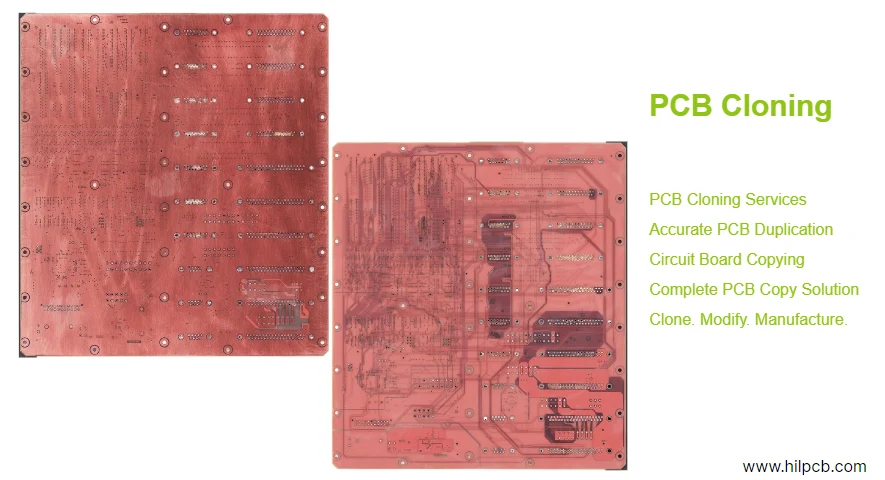
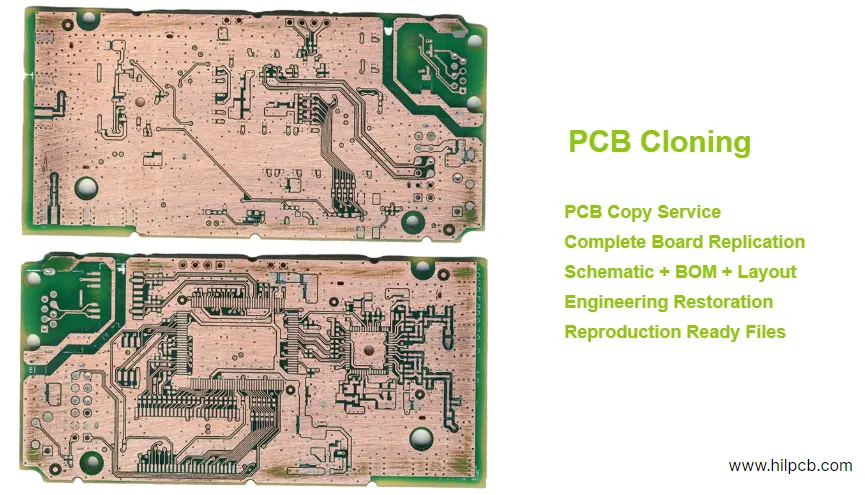
PCB Cloning: Creates duplicate board from physical sample. No original files. Focus on exact replication. Output: Gerber files and BOM for manufacturing identical copies.
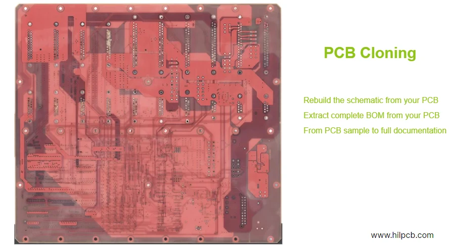
PCB Reverse Engineering: Creates complete design documentation including schematics through PCB reverse engineering. More comprehensive than cloning. Output: Schematics, layout files, component specifications, design documentation enabling modifications.
PCB Copying: Manufacturing term for producing additional boards from sample through PCB copying. Often used interchangeably with cloning. Implies production focus rather than design focus.
PCB Replication: Scaling proven design to production volumes with PCB replication. Original design files exist. Focus on manufacturing optimization, not reverse engineering.
Why Professional Cloning Services Exist
Given technical complexity, most companies outsource cloning rather than building internal capability:
Economic Factors:
- Capital equipment investment prohibitive for occasional needs
- Experienced engineering staff expensive and difficult to retain
- Component sourcing networks take years to develop
- Legal expertise required for IP navigation
Technical Expertise Required:
- Materials science knowledge for board construction
- RF engineering for high-frequency designs
- Package technology understanding for modern components
- Manufacturing process knowledge for PCB rework
Service Provider Advantages:
- Amortize equipment costs across many projects
- Maintain specialized engineering expertise
- Establish component sourcing networks
- Navigate legal and IP issues regularly
Understanding PCB cloning technology, methods, and limitations helps you evaluate service providers, understand realistic timelines and costs, and determine when cloning makes sense versus alternatives like repair or redesign.
Need professional PCB cloning services? Our technical team uses the methods described here to deliver accurate board replication for legitimate maintenance, repair, and legacy equipment support.
Professional equipment • Experienced engineers • Legal compliance • Quality assurance