Original design files lost. Previous supplier went out of business. Legacy product needs continuation but documentation vanished. Competitor's design requires analysis. These situations demand reverse engineering - recreating schematics and layouts from physical boards when original data doesn't exist or isn't accessible.
HILPCB reverse engineering services recreate complete design data from existing boards, enabling reproduction, modification, and ongoing support for products when original documentation is unavailable.
When Reverse Engineering Becomes Necessary
Design data disappears for various reasons. Understanding common scenarios helps plan appropriate responses when facing missing documentation challenges.
Obsolete Product Support
Manufacturing equipment from 15 years ago fails. Replacement boards unavailable - original manufacturer discontinued product line or went bankrupt. Reverse engineering existing boards enables continued production without redesigning entire system.
Medical devices face similar challenges. FDA-approved devices require maintaining exact designs. Component obsolescence forces changes but modifying FDA documentation costs millions. Reverse engineering existing boards plus component substitution maintains approval while enabling continued manufacturing through PCB cloning services.
Industrial controls present decades-long support requirements. Plants running 24/7 cannot tolerate equipment downtime. Original supplier support ended years ago. Reverse engineering enables maintaining spare board inventory supporting equipment throughout its operational life, often complemented by professional PCB repair capabilities.
Lost or Inaccessible Design Data
Fire destroys company records. Hard drives crash without backups. Previous engineer left and took files. Contract manufacturer refuses releasing design data claiming ownership. Reverse engineering recovers design information from physical boards.
Acquisitions and mergers create documentation gaps. Acquired company's design records incomplete or incompatible formats. Reverse engineering existing production boards establishes baseline documentation for ongoing support and future modifications, supporting efficient PCB development cycles.
Competitive Analysis and Design Validation
Understanding competitor implementations requires board-level analysis. Which components do they use? How do they route high-speed signals? What power supply architecture? Reverse engineering reveals design approaches and component selections informing your development decisions.
Design validation for critical applications benefits from reverse engineering analysis. Does as-built board match design documentation? Did manufacturing substitutions occur? Are there undocumented modifications? Physical board analysis confirms actual implementation versus documentation through comprehensive PCB inspection techniques.
The Reverse Engineering Process
Systematic approach ensures complete and accurate design recreation. Skipping steps risks missing critical details that cause reproduction failures.
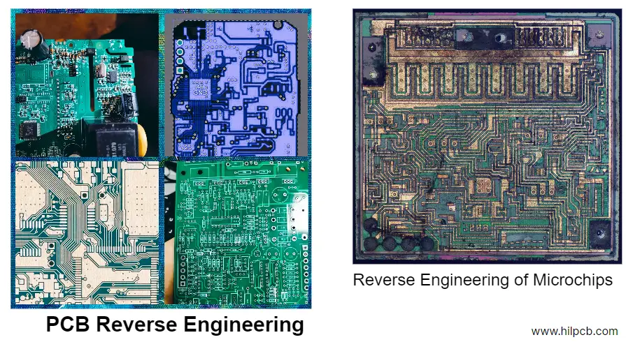
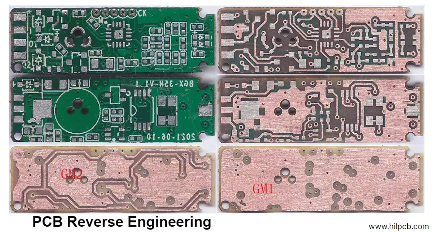
Physical Board Documentation
High-resolution photography captures both sides and component details:
- Overall board images showing component layout and arrangement
- Close-up images of every component showing markings and orientation
- Connector pinouts and mechanical features
- Any modifications, rework, or hand-added components
Board measurements document physical characteristics:
- Overall dimensions and board thickness
- Hole locations and diameters
- Component placement locations
- Connector positions and orientations
Component Identification and Bill of Materials
Every component gets identified and cataloged:
- Part numbers from component markings
- Component values (resistors, capacitors, inductors)
- IC datasheets and specifications
- Obsolescence status and availability
- Alternative component options for obsolete parts
Creating BOM includes:
- Complete component list with reference designators
- Manufacturer part numbers and descriptions
- Package types and footprints
- Quantity requirements
- Sourcing information and lead times
Obsolete component handling requires planning. Original parts unavailable? Identify modern equivalents with similar specifications. Our PCB engineering team evaluates alternatives ensuring electrical compatibility.
Layer Stack-Up Determination
Multi-layer boards require determining internal layer configuration:
- X-ray imaging reveals internal traces and vias
- Careful board sectioning exposes layer structure
- Ohmmeter testing maps connectivity between layers
- Analysis determines signal, power, and ground plane assignments
2-4 layer boards: Relatively straightforward determination 6+ layer boards: Complex analysis requiring experienced interpretation HDI boards with microvias: Most challenging requiring specialized equipment
Circuit Tracing and Schematic Capture
Methodical process traces every connection:
- Start with power supply section identifying voltage rails
- Trace power distribution to each IC and component
- Map signal connections between components
- Identify feedback loops and control paths
- Document test points and interfaces
Schematic capture using professional CAD tools:
- Organized by functional blocks (power, processor, I/O, etc.)
- Hierarchical sheets for complex designs
- Net naming following logical conventions
- Component values and part numbers annotated
Multi-layer boards present challenges:
- Internal connections not visible from surface
- Via tracing requires continuity testing
- Power and ground planes need careful mapping
- Signal layer assignments must be determined
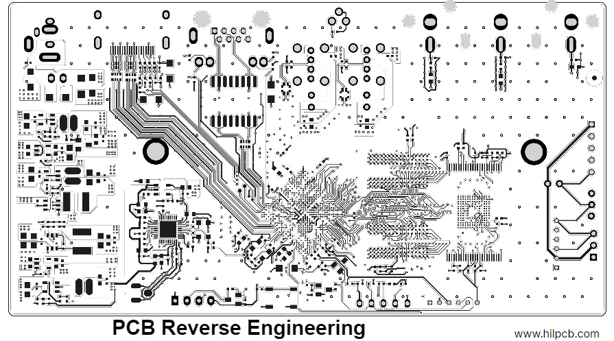
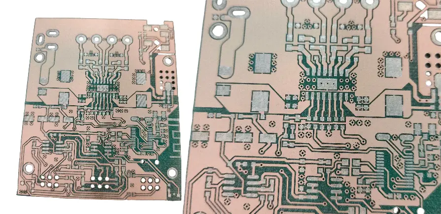
PCB Layout Recreation
Gerber file generation from physical board measurements:
- Scan both sides capturing trace patterns
- Import scans into CAD software
- Manually trace or use auto-routing following original patterns
- Place components matching physical locations
- Verify pad sizes and trace widths
Design rule verification ensures manufacturability:
- Minimum trace widths and spacings
- Annular rings around drilled holes
- Solder mask and silkscreen clearances
- Via sizes and spacing
Layout recreation approaches:
- Exact replication: Match original layout precisely including component placement and trace routing, ideal for PCB copying requirements
- Optimized recreation: Improve layout while maintaining functionality (better routing, updated components, cost reduction)
Choice depends on requirements. Exact replication for regulatory-approved designs. Optimized recreation for commercial products enabling improvements.
Complexity Factors Affecting Cost and Timeline
Not all boards present equal challenges. Understanding complexity factors helps estimate effort and set realistic expectations.
Simple Boards (1-2 Weeks)
- 2 layers with minimal components (<50)
- Through-hole technology predominant
- Simple circuits (power supplies, basic control)
- Readily available components
- No high-frequency or precision analog circuits
Moderate Complexity (2-4 Weeks)
- 4 layers with mixed SMT and through-hole
- 50-200 components
- Microcontroller or simple digital logic
- Standard interfaces (RS232, USB, Ethernet)
- Some component identification challenges
High Complexity (4-8+ Weeks)
- 6+ layers with blind/buried vias
- 200+ components including fine-pitch BGAs
- Complex digital (FPGAs, processors) or high-speed analog
- Multiple power domains and voltage rails
- Obsolete components requiring research
- Undocumented modifications or rework visible
Factors Increasing Difficulty:
Component Issues:
- Unmarked or house-numbered components requiring extensive research
- Obsolete parts with no direct replacements
- Potted or conformal coated assemblies preventing inspection
- Components removed or damaged on sample boards
Board Construction:
- 8+ layer boards with complex stackups
- HDI with laser-drilled microvias
- Rigid-flex boards with multiple fold regions
- Embedded components within board structure
Circuit Complexity:
- High-speed digital requiring impedance control understanding
- Precision analog with tight matching requirements
- RF circuits where layout affects performance
- Safety-critical or regulatory-approved designs requiring exact replication
Legal and Ethical Considerations
Reverse engineering exists in legal gray areas. Understanding boundaries prevents problems while enabling legitimate applications.
Legal Reverse Engineering
Generally permitted for:
- Products you own for interoperability, maintenance, or compatibility
- Competitive analysis and design education
- Supporting obsolete or unsupported products
- Recovering lost design data for products you designed
Prohibited Activities:
Avoid:
- Violating patents, copyrights, or trade secrets
- Circumventing security measures or DRM
- Producing counterfeit products or trademark violations
- Reverse engineering under NDA prohibiting such activity
Best Practices:
- Document legitimate business purpose
- Work from products legally purchased
- Avoid copying exact layouts when alternatives exist
- Respect intellectual property rights
- Consult legal counsel for sensitive situations
HILPCB performs reverse engineering for legitimate purposes supporting product maintenance, interoperability, and design education. We decline projects appearing to enable IP theft or counterfeit production.
From Reverse Engineering to Production
Complete design data enables multiple outcomes depending on objectives.
Exact Reproduction
Maintaining identical functionality and form factor:
- Gerber files matching original layout
- BOM with exact or equivalent components
- Assembly drawings showing placement and orientation
- Test procedures verifying functionality through rigorous PCB testing
Applications include:
- Spare parts for legacy equipment
- Continued production of discontinued products
- Warranty support when original supplier unavailable
Our PCB replication services enable scalable production once designs are fully documented.
Design Improvement and Modernization
Using original as starting point for enhancements:
- Replace obsolete components with modern equivalents
- Improve layout for better manufacturability
- Add features or interfaces not in original
- Cost reduction through design optimization
Benefits include:
- Extended product life with available components
- Performance improvements with updated technology
- Cost savings from manufacturing improvements
- Feature additions meeting current requirements
When design modifications are needed after production, our PCB rework capabilities support efficient implementation of engineering changes.
Competitive Analysis Integration
Information gathered informs your product development:
- Component selections and why competitors chose them
- Design approaches for similar functionality
- Cost structures based on BOM analysis
- Performance trade-offs evident from implementation
Use insights improving your designs without copying, respecting IP boundaries while learning from market.
Reverse Engineering Deliverables
Complete documentation package enables reproduction and modification:
Design Files:
- Schematic in CAD format (Altium, Cadence, KiCAD, etc.)
- PCB layout files with all layers
- Gerber files for manufacturing
- Assembly drawings
Bill of Materials:
- Complete component list with specifications
- Manufacturer part numbers and alternatives
- Sourcing information and availability
- Obsolescence status and replacement options
Documentation:
- Reverse engineering methodology and process
- Design notes explaining circuit functionality
- Component identification challenges and resolutions
- Manufacturing notes and special requirements
Manufacturing Support:
- PCB manufacturing setup and production
- Component sourcing and procurement
- PCB assembly services
- Testing and validation
From design recreation through manufacturing support, HILPCB reverse engineering services provide complete solutions for products requiring continued support. Visit www.hilpcb.com/en/ to discuss your reverse engineering needs.