Finding a capable PCB manufacturer separates successful blog from development disasters. While thousands claim "professional PCB manufacturing" or "certified circuit board manufacturing," few possess genuine technical capability, quality systems, and production scale. Poor manufacturer selection creates problems: boards fail signal integrity requirements from inadequate processes, quality defects generate field failures, limited technology constrains future designs, and unreliable delivery disrupts production schedules.
Manufacturing sophistication determines design feasibility. Advanced PCB manufacturers handle HDI with 2/2mil traces and microvias. High-frequency PCB manufacturers process Rogers, Taconic, and Arlon materials correctly. Automotive PCB manufacturers maintain IATF 16949 certification. Medical device PCB manufacturers comply with ISO 13485. Contract PCB manufacturers scale from prototypes to millions of boards. Small batch PCB manufacturers maintain quality at low volumes.
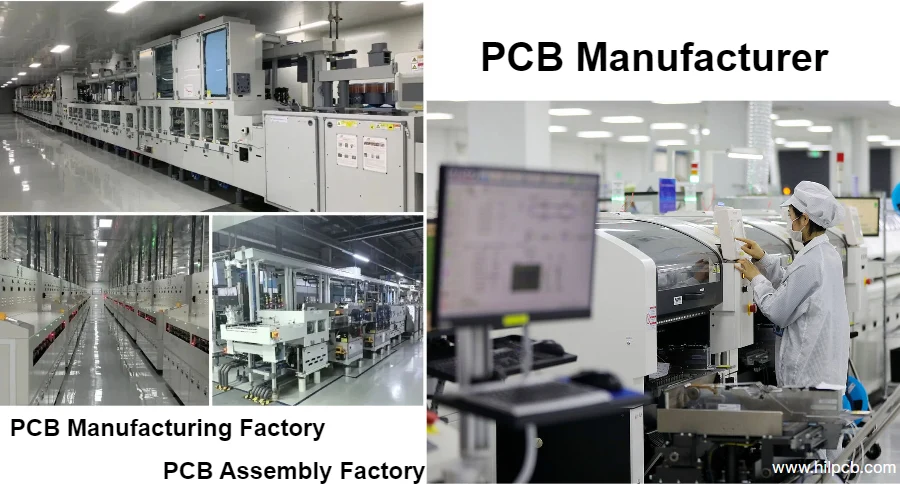
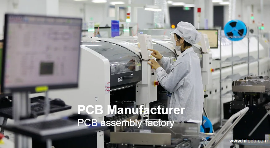
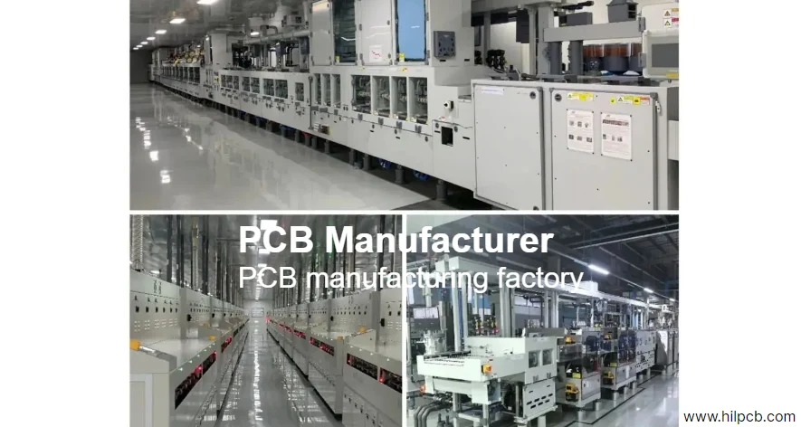
Highleap PCB Factory (HILPCB) operates as a professional China PCB manufacturer with verified capabilities across all major technologies. Our manufacturing credentials include ISO 9001/AS9100/ISO 13485 certifications, complete technology range (2-64 layers, rigid/flex/HDI, specialty materials), advanced equipment (LDI, laser drilling, automated testing), and integrated PCB Assembly services backed by our comprehensive PCB Factory infrastructure.
PCB Manufacturer Capability Tiers
Manufacturing sophistication varies dramatically. Understanding capability levels prevents mismatched expectations across different PCB Manufacturing operations.
Basic PCB Manufacturers (Limited Capability):
- Layer range: 1-10 layers, primarily simple rigid boards
- Feature sizes: 5/5mil traces/spaces, standard processes only
- Materials: Standard FR4 only, no specialty substrates
- Via technology: Through-holes only, no HDI capability
- Applications: Simple consumer electronics, hobby projects
- Limitations: Cannot handle complex designs, limited quality systems
Intermediate PCB Manufacturers (Standard Production):
- Layer range: 2-16 layers with conventional stackups
- Feature sizes: 3/3mil traces/spaces with film-based imaging
- Materials: Standard and high-Tg FR4, limited specialty materials
- Via technology: Through-holes plus basic blind/buried vias
- Quality systems: ISO 9001, basic IPC compliance
- Applications: Industrial controls, telecommunications, automotive Tier 2
Advanced PCB Manufacturers (Full Capability):
- Layer range: 2-64 layers with sequential lamination
- Feature sizes: 2/2mil traces with laser direct imaging
- Materials: Complete range—FR4, Rogers, Taconic, Arlon, polyimide, metal core, ceramics
- Via technology: HDI with any-layer microvias, stacked/staggered configurations
- Quality systems: ISO 9001, AS9100, ISO 13485, IATF 16949, IPC Class 3
- Applications: Aerospace, medical, automotive Tier 1, 5G infrastructure, high-performance computing
Critical Manufacturing Processes
Process maturity determines whether manufacturers deliver consistent results or struggle with variation and defects across PCB Fabrication operations.
Advanced Imaging & Patterning:
- Laser Direct Imaging (LDI): Computer-controlled lasers write 2mil traces directly, eliminating film errors
- Film-based imaging: Traditional method for standard geometries (4-5mil minimum)
- Registration control: ±50µm layer-to-layer alignment for HDI and fine-pitch assembly
- Automated Optical Inspection (AOI): Scans every layer for defects before lamination
Precision Drilling Technologies:
- Mechanical drilling: Multi-spindle CNC systems, 0.15mm minimum diameter, ±25µm accuracy
- Laser drilling (CO2): Creates standard microvias 50-150µm for HDI
- UV laser drilling: Finer microvia control for advanced applications
- Back-drilling: Removes via stubs for high-speed signal integrity
- Aspect ratio capability: Up to 16:1 for specialized applications
Controlled Plating Processes:
- Electroless copper: Deposits conductive seed layer in drilled holes
- Electrolytic plating: Builds copper thickness with automated current density control
- Thickness monitoring: Real-time measurement ensures uniform distribution
- Via filling: Copper or resin fill for planar surfaces, via-in-pad applications
Sequential Lamination:
- HDI build-up: Multiple lamination cycles create complex layer structures
- Rigid-flex construction: Bonds rigid sections with flexible interconnects
- Material-specific profiles: Rogers at reduced temperatures, polyimide extended cure
- Vacuum lamination: Prevents voids, ensures uniform bonding
Surface Finish Application:
- ENIG (Electroless Nickel Immersion Gold): Best for fine-pitch, wire bonding, shelf life
- Immersion Silver: Excellent solderability, cost-effective
- OSP (Organic Solderability Preservative): Lowest cost, eco-friendly
- Immersion Tin: Flat surface for press-fit applications
- HASL (Hot Air Solder Leveling): Traditional, long shelf life
Our advanced manufacturing processes are integrated with rapid PCB Prototyping capabilities for seamless development cycles.
Specialty Material Manufacturing Expertise
Standard FR4 processing represents baseline capability. Advanced manufacturers distinguish through specialty material proficiency as part of comprehensive PCB Services.
High-Frequency Material Processing:
- Rogers manufacturing: RO4003C/4350B (1-10 GHz), RT/duroid 5880/6002 (10+ GHz)
- Taconic processing: TLY-5, RF-35 for military/aerospace RF systems
- Arlon fabrication: 25N, DiClad for high-reliability applications
- Modified processes: Lower lamination temps (prevents degradation), specialized drilling (prevents smearing), controlled etching (accurate trace geometry)
- Impedance control: ±3Ω tolerance with TDR/VNA verification
Metal Core PCB Manufacturing:
- Aluminum core: 1-10 W/mK thermal conductivity, cost-effective
- Copper core: 200-400 W/mK for maximum heat dissipation
- Specialized lamination: Bonds circuit layers to metal base without damage
- Thermal via processing: Creates heat transfer paths through dielectric
- Applications: LED lighting, power electronics, motor drives
Ceramic PCB Manufacturing:
- Alumina (Al₂O₃): 96-99.6% purity, excellent electrical insulation
- Aluminum Nitride (AlN): 170-200 W/mK thermal conductivity
- Thick-film/thin-film: HTCC and LTCC technologies
- Applications: Power modules, RF/microwave, high-reliability aerospace
Polyimide & Flex Manufacturing:
- Rigid polyimide: Glass transition >250°C for extreme temperatures
- Flexible polyimide: Kapton-based for dynamic flexing applications
- Rigid-flex constructions: Combines rigid sections with flex interconnects
- Extended cure cycles: Achieves full polymerization without material stress

Quality Systems & Certifications
Quality certifications indicate minimum standards, but implementation depth separates compliant manufacturers from quality leaders in PCB Production environments.
ISO 9001:2015 (Quality Management Foundation):
- Basic quality management system—necessary but insufficient for advanced manufacturing
- Process documentation, corrective action systems, continuous improvement
- Verify with current certificate and recent audit reports
IATF 16949 (Automotive Quality):
- Automotive-specific requirements: PPAP, APQP, FMEA, control plans
- Mandatory for automotive Tier 1/2 suppliers
- Includes ISO 9001 requirements plus automotive additions
- Verify through IATF database, request PPAP documentation examples
ISO 13485 (Medical Device Manufacturing):
- Medical device-specific quality management
- Risk management, design control, validation protocols
- Traceability requirements, sterilization compatibility
- Verify current certificate, request design history file examples
AS9100 (Aerospace Manufacturing):
- Aerospace-specific requirements beyond ISO 9001
- Configuration control, counterfeit prevention, first article inspection
- Critical for aerospace and defense applications
- Verify with NADCAP or AS9100 certification database
IPC Standards Implementation:
- IPC-A-600: Acceptability criteria for PCB fabrication (Class 2 vs Class 3)
- IPC-6012: Performance specifications for rigid boards
- IPC-A-610: Acceptability of electronic assemblies
- Request sample inspection reports showing actual implementation
Engineering Support Capabilities
Technical collaboration distinguishes manufacturing partners from transactional vendors across all PCB Design integration points.
Design for Manufacturing (DFM) Analysis:
- Automated checking: Verifies clearances, drill sizes, aspect ratios
- Engineering review: Experienced designers examine manufacturability concerns
- Material recommendations: Suggests optimal substrates balancing performance and cost
- Stackup optimization: Refines layer arrangement for impedance control and signal integrity
Process Development:
- New material qualification: Tests and optimizes parameters for novel substrates
- Custom stackup development: Designs layer arrangements for specific requirements
- Yield optimization: Refines processes to maximize first-pass success
- Prototype-to-production: Ensures consistency as quantities scale
Technical Consultation:
- Material selection: Guides choices based on application requirements
- Impedance calculation: Provides stackup design for controlled impedance
- Thermal analysis: Evaluates heat spreading and cooling requirements
- Failure analysis: Investigates defects to address root causes
HILPCB Manufacturing Excellence
Complete Technology Range:
- 2-64 layer capability with sequential lamination
- Line width/space: 2/2mil minimum (HDI), 3/3mil standard production
- All materials: FR4 to Rogers/Taconic to ceramics, metal core
- HDI, rigid-flex, heavy copper (3-20oz), specialty constructions
Advanced Equipment:
- Laser direct imaging (LDI) systems for fine-pitch
- Laser drilling (CO2 and UV) for microvias
- Sequential lamination presses for complex stackups
- Automated testing: flying probe, impedance (TDR/VNA), X-ray
Quality Certifications:
- ISO 9001:2015 quality management (current)
- AS9100 aerospace manufacturing (current)
- ISO 13485 medical device fabrication (current)
- IATF 16949 automotive quality (current)
- IPC-A-600/6012 Class 2 and Class 3 compliance
Integrated Services:
- PCB fabrication + assembly under one roof
- Component sourcing from authorized distributors
- Design for Manufacturing (DFM) analysis
- Prototype to production scalability
- Supply chain management and logistics
From standard rigid boards to complex HDI, rigid-flex, and specialty material processing, HILPCB delivers as a professional China PCB manufacturer with verified quality, advanced capability, and reliable execution. Our position as a comprehensive PCB Company enables seamless coordination across all manufacturing stages. Advanced PCB Solutions ensure that even the most demanding applications receive expert attention throughout production.
Frequently Asked Questions
Q1: How do I verify a PCB manufacturer's certifications are legitimate? Request certificate copies with registration numbers and expiration dates. Verify with issuing organizations—ISO can be checked through registrar databases; IATF 16949, AS9100, ISO 13485 have online verification. Request recent audit reports, not just certificates. Legitimate manufacturers readily provide documentation.
Q2: What's the difference between a PCB manufacturer and a PCB broker? Manufacturers own fabrication equipment and directly control processes. Brokers coordinate production through third parties. Manufacturers typically offer better technical support, process control, and problem resolution for complex boards. Brokers may access multiple manufacturing sources but add margin without adding value for most applications.
Q3: Can China PCB manufacturers match domestic quality standards? Top-tier China manufacturers meet or exceed domestic quality with advanced equipment (LDI, laser drilling, automated inspection) and certifications (ISO 9001, AS9100, ISO 13485, IATF 16949). Key is thorough vetting—verify certifications, request samples, check references, conduct trial orders. Quality varies widely; choose carefully.
Q4: What capabilities should I verify before selecting a PCB manufacturer? Confirm maximum layer count, minimum feature sizes (trace/space), supported materials beyond FR4, HDI capability (microvia technology), specialty processes (blind/buried vias, heavy copper, metal core), and certifications matching your industry. Request board examples with photos showing actual production quality. Conduct trial orders before production commitment.