
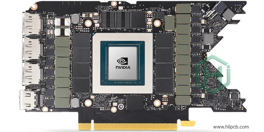
A PCB video card is the multilayer assembly connecting a GPU, graphics memory, power converters, host/display interfaces, clocks, sensors, and cooling hardware. It supports those devices but cannot alone guarantee clock speed, overclocking margin, acoustic behavior, certification, or finished-card performance.
Key Takeaways
- PCIe, GDDR, DisplayPort, HDMI, clocks, and management buses need separate constraints.
- Layer count, material, copper, and vias follow released electrical, mechanical, and process requirements.
- GPU heat normally exits through the package top, TIM, and heatsink or cold plate; the PCB mainly spreads local VRM and memory heat.
- VRM phase count follows current, transients, efficiency, thermals, control architecture, and area.
- Release evidence must cover stackup, impedance, PDN, channels, assembly, functional test, and ownership.
Table of Contents
- What Does a PCB Video Card Actually Do?
- Use an Interface-to-Evidence Matrix
- Choose Stackup, Material, and Copper Together
- Design GPU Power Without a Fixed Phase Count
- Separate GPU Cooling from PCB Heat Spreading
- Plan Assembly and Inspection Around the Packages
- Validate from Bare Board to Finished Card
- Diagnose Common GPU Board Failure Modes
- PCB Video Card RFQ Checklist
- Reference Standards and Responsibility Boundaries
- How HILPCB Can Support a GPU PCB Build
- Frequently Asked Questions
What Does a PCB Video Card Actually Do?
The board combines BGA escape, high-speed links, low-voltage/high-current power, mechanical support, assembly geometry, and cooling interfaces. It carries the GPU, GDDR, converters, clocks, PCIe edge fingers, display connectors, fan control, sensors, protection, and firmware storage.
These functions compete for space and process margin. More copper lowers resistance but complicates fine-line etching, impedance, resin fill, and reflow. More layers improve routing and references but add registration, lamination, cost, and lead-time risk. Thus “8–12 layers,” “2 oz,” and “85 ohms” are not universal specifications; the released architecture determines them.

Use an Interface-to-Evidence Matrix
Assign every interface its own source of truth. When limits are access-controlled, the design team must release them rather than ask a fabricator to infer them.
| Interface or circuit | Primary constraint source | PCB concerns | Release evidence |
|---|---|---|---|
| PCI Express host link | GPU data; PCI-SIG Base/CEM | Impedance, loss, returns, transitions, AC coupling | Rules, stackup, models, channel/coupon plan |
| GDDR memory | Exact GPU/memory data; JEDEC | Topology, skew groups, references, crosstalk, package delay | Pin data, groups, timing budget, simulation |
| DisplayPort or HDMI | GPU data; VESA/HDMI specification | Launch, ESD, loss, skew, returns | Rules, approved parts, compliance plan |
| GPU and memory rails | GPU, regulator, and power-stage data | Target impedance, transients, phases, loops, sensing | Rail/load budget, PDN model, limits |
| Reference clocks | Source and receiver data | Jitter, isolation, returns, termination | Clock tree, budget, scope method |
| I2C, SPI, fan and sensors | Datasheets and firmware | Pull-ups, domains, sequence, access | Power-state table, functional test |
PCIe 5.0 operates at 32 GT/s per lane, while Micron's current GDDR7 information describes up to 32 Gb/s per pin with PAM3. Equal headline numbers do not make their routing interchangeable. Device and standard data must define topology, impedance, and timing. Express matching as a skew budget including package delay; blanket “±5%” matching may be too loose or unnecessarily tight.
Before layout release, convert the matrix into a controlled constraint ledger. For each row, name the document revision, owner, nets, numerical limits, model files, simulation status, planned measurement, and waiver authority. If a device or connector changes, reopen only the affected rows and their dependent tests. This makes substitutions auditable and prevents an unverified “equivalent” part from silently changing loss, pin delay, power sequence, or compliance scope.
Choose Stackup, Material, and Copper Together
Converge layer count and material from routing density, reference continuity, loss, rail geometry, thickness, vias, and fabricator capability. A premium laminate name is not evidence; use controlled dielectric, roughness, construction, and channel data.
| Decision | Choose more capability when | Watch the tradeoff |
|---|---|---|
| More layers | Escape, references, or power cannot fit cleanly | Cost, registration, lamination, lead time |
| Lower-loss dielectric | Modeled channel loss lacks margin | Availability, press behavior, Dk/Df variation, cost |
| HDI/via-in-pad | Fine-pitch escape or transitions require it | Fill/planarization, microvia reliability, yield |
| Backdrilling | Modeled via stubs degrade a channel | Drill tolerance, residual stub, coupons |
| Heavier copper | DC loss, current density, or spreading justifies it | Fine lines, impedance, resin fill, balance |
| Hybrid material | Only selected layers need lower loss | Lamination, CTE, procurement, qualification |
Heavier copper may suit selected power layers, but 2–4 oz everywhere can conflict with dense GDDR escape and impedance geometry. Before routing, obtain a proposed stackup showing finished copper, dielectrics, materials, impedance structures, tolerances, and coupons.
Design GPU Power Without a Fixed Phase Count
A low-voltage GPU rail makes parasitic inductance and control response as important as ampacity. Phase count follows maximum/transient current, allowed ripple and droop, switching frequency, stage rating, efficiency, thermals, control law, area, and cost—not a fixed 10–20 phase rule.
For every rail, release input range, voltage tolerance, load steps, slew rate, sequence, protection, and modes. Calculate target impedance from permitted disturbance and current demand. Keep input switching loops compact, switch nodes controlled, decoupling close, remote sense quiet, and power/ground transitions low-inductance; then measure phase sharing and temperature.
Coil whine occurs when electrical excitation drives mechanical vibration in inductors or capacitors. Components, load pattern, assembly, mounting, and enclosure acoustics contribute. Layout may alter excitation but cannot guarantee silence.
Separate GPU Cooling from PCB Heat Spreading
The main GPU heat path normally runs from die/package top through a thin TIM into a heatsink, vapor chamber, or cold plate. NVIDIA module guidance similarly treats package contact, TIM bondline, pressure, board flex, and system qualification as controlled responsibilities.
PCB planes and thermal vias help VRM, inductor, memory, and local spreading paths but do not replace the GPU cooler. Shared thermal pads need tolerance and pressure analysis because GPU heat can warm neighboring parts.
Release outline, thickness, keep-outs, mounting tolerances, connector datum, component heights, pad compression, fastener sequence, board-strain limit, and card support. Evaluate the full cooler-to-bracket/chassis load path, not board thickness alone.

Plan Assembly and Inspection Around the Packages
BGAs, bottom-terminated power parts, small passives, thermal pads, and edge fingers create different risks. Control moisture, stencil apertures, paste, placement, support, reflow, warpage, and handling for the actual package mix.
Use 3D SPI for print, AOI for visible features, and specified X-ray for hidden joints. These checks do not prove channel performance. The reliability plan may add microsection, dye-and-pry, cleanliness, cycling, vibration, or strain tests.
Bare-board test checks opens/shorts; coupons verify fabricated impedance structures. When loss or discontinuities matter, release the TDR/VNA method, fixture, de-embedding, range, limits, and sampling.
Validate from Bare Board to Finished Card
Validation should climb in controlled gates so a firmware or benchmark result cannot hide a manufacturing defect.
| Gate | Main checks | What a pass does not prove |
|---|---|---|
| 1. Fabricated PCB | Dimensions, stackup records, coupons, continuity/isolation, visual and microsection evidence as specified | Assembly quality or channel compliance |
| 2. Unpowered PCBA | SPI/AOI/X-ray results, polarity, resistance-to-ground, shorts, workmanship | Correct sequencing or rail dynamics |
| 3. Current-limited power-up | Input current, rail order, voltage, ripple, clocks, reset, thermal survey | Full-load transient or interface margin |
| 4. Device bring-up | GPU identification, firmware access, memory initialization, sensors and fans | Rated-speed channel or thermal capability |
| 5. Electrical margin | PDN transient tests, channel/eye/BER tests, display-interface checks | Product certification outside the tested configuration |
| 6. System stress | Workload, thermal soak, power cycling, acoustics, mechanical and environmental tests | Untested use cases or lifetime beyond the plan |
| 7. Compliance/release | Applicable PCIe/display/EMC/safety program and controlled evidence | Future revisions without requalification |
Record revision, BOM option, firmware/driver, test version, fixture, limits/results, ambient, cooler, and serial number. “Benchmark passed” without these identities is not reproducible.
Release criteria should also state who may disposition a failure. A fabricator can confirm a coupon or construction deviation; the design authority must judge whether altered channel, power, thermal, firmware, or compliance behavior is acceptable. Keep rework history linked to the unit so a later pass does not erase the original defect signal.
Diagnose Common GPU Board Failure Modes
| Symptom | Plausible causes | First useful evidence |
|---|---|---|
| Card not detected | Slot power, reset/clock, edge fingers, firmware, PCIe lane fault | Rail sequence, reference clock, reset, link-training log |
| Memory errors | Wrong topology/rules, solder defect, rail noise, timing or temperature | Per-channel errors, X-ray, memory rail waveform, thermal map |
| Crash under load | PDN transient, thermal throttling, assembly intermittency, firmware | Rail droop/current, junction and component temperatures, event log |
| One display output fails | Connector/ESD assembly, lane routing, firmware, cable or sink | Connector inspection, lane waveform, known-good cable/display |
| Hot VRM phase | Current imbalance, layout resistance, component or cooling variation | Phase current/temperature map, switching waveforms, copper review |
| Audible noise | Magnetics/capacitor vibration excited by operating mode | Frequency/load correlation, component-level acoustic isolation |
| PCIe works only at lower generation | Loss, reflection, via/connector transition, reference or clock issue | Negotiated link log, TDR/VNA/eye evidence, stackup and coupon data |
PCB Video Card RFQ Checklist
Design and fabrication package
- schematic, manufacturing data, drawings, netlist, revision and panel requirements;
- stackup, thickness, finished copper, material/electrical targets, impedance table and coupons;
- interface generations/rates, routing rules, models, via/backdrill requirements and evidence;
- dimensions, edge fingers, mounting datum, tolerances, keep-outs, cooler/backplate and strain limits.
BOM and assembly package
- approved BOM, lifecycle/substitution rules and customer-supplied parts;
- centroid, assembly/orientation/package data and moisture handling;
- stencil, reflow, support, inspection, cleaning and coating requirements;
- programming, image hashes, security and serialization.
Test and acceptance package
- rail sequence, current limits, power-up, fixtures and safe states;
- board/coupon, inspection, functional, interface, PDN, thermal, acoustic and reliability tests;
- limits, sampling, retest/repair, golden units, traceability and retention;
- compliance owner, lab evidence, deviations and requalification triggers.
Reference Standards and Responsibility Boundaries
Applicable references may include:
- PCI Express Base Specification and Card Electromechanical Specification, PCI-SIG
- JESD250, GDDR6 SGRAM, JEDEC
- JESD239, GDDR7 SGRAM, JEDEC
- DisplayPort Standard, VESA
- HDMI Specification, HDMI Forum or HDMI Licensing Administrator as applicable
- IPC-2221 and IPC-2222 for PCB design requirements as invoked
- IPC-6012 for rigid printed board qualification and performance as invoked
- J-STD-001 and IPC-A-610 for soldering and assembly acceptance as invoked
Use owner-invoked revisions and criteria. The card designer owns components, constraints, firmware, cooling, safety, compliance, performance, and qualification. The PCB/PCBA supplier owns quoted fabrication, assembly, inspection, test, records, and deviations. Build-to-data does not certify the finished card.
How HILPCB Can Support a GPU PCB Build
HILPCB can review dense HDI PCB, high-speed PCB, multilayer PCB, and SMT assembly manufacturability. Quote material, stackup, coupons, vias/backdrill, edge fingers, BGA inspection, programming, fixtures, measurements, and reliability tests explicitly.
Use the quote page and request proposed construction, exceptions, dependencies, test coverage, evidence, lead-time drivers, and change-control boundaries.
Frequently Asked Questions
How many layers does a PCB video card need?
No universal count exists. Escape, channels, references, power, thickness, vias, and fabrication limits determine it.
Is every high-speed pair on a graphics card 85 ohms?
No. Their device and standard requirements differ. Release interface-specific impedance and timing rules.
Does thicker copper always improve a GPU PCB?
No. It lowers resistance but complicates fine lines, impedance, resin fill, balance, cost, and yield.
Can a PCB manufacturer guarantee higher GPU boost clocks?
No. Silicon, firmware, power, cooling, workload, and system limits govern clocks. A supplier can verify only agreed PCB/PCBA requirements.
Can PCB layout eliminate coil whine?
No. Components, load patterns, mounting, control behavior, and enclosure acoustics also govern it.
Conclusion
A production-ready PCB video card needs interface-specific constraints, a co-designed stackup/PDN, direct package cooling, package-aware assembly, staged validation, and frozen responsibility boundaries—not fixed layer, impedance, phase, or copper recipes.