
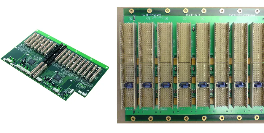
AI server backplane potting is the controlled placement of a cured compound around selected PCB regions for environmental, mechanical or thermal protection. The same material can obstruct a connector, load a solder joint, alter a surface electromagnetic field and prevent repair.
Key Takeaways
- Do not pot an entire AI server backplane by default. Start with the failure mode, then protect the smallest region that closes the risk.
- Keep compound away from connector mating interfaces, press-fit zones, optical ports, airflow, test points and field-replaceable parts unless explicitly qualified.
- Stress depends on modulus, coefficient of thermal expansion (CTE), cure shrinkage, temperature, bond area and constraint—not material family alone.
- Thermal compound needs a controlled bond line to a defined sink; filling air space is not a thermal design.
- Supplier dielectric data measured at 1 MHz cannot be inserted directly into a PCIe or CXL channel model. Characterize the cured production material at relevant frequencies and temperatures.
- Complete inspectability and electrical tests before encapsulation, then compare TDR, VNA or link-level results before and after the process when the compound enters a high-speed launch field.
- Freeze resin, hardener, mix ratio, dispense geometry and cure as one qualified system. A faster substitute is a design change.
Table of Contents
- Should an AI Server Backplane Be Potted?
- Potting vs Encapsulation vs Conformal Coating
- Choose Epoxy, Silicone or Polyurethane by Risk
- Protect High-Speed Connectors and Signal Fields
- Build a Real Thermal Path
- Control Mechanical Stress and Cure Geometry
- Design the Manufacturing Process Around Evidence
- Validate Before and After Encapsulation
- Diagnose Common Potting Failures
- AI Server Backplane Potting RFQ Checklist
- Reference Standards and Responsibility Boundaries
- How HILPCB Supports Selective Encapsulation
- FAQ
- Conclusion
Should an AI Server Backplane Be Potted?
First decide whether potting controls a documented failure mode. Data-center equipment prioritizes airflow, connector serviceability, field replacement and upgrades, which often conflict with encapsulation.
Use this decision matrix before releasing a drawing:
| Decision factor | Potting may help when | Potting may create a larger risk when | Evidence required |
|---|---|---|---|
| Moisture, dust or chemicals | A localized assembly has a defined ingress path | Protection blocks inspection or cooling in a controlled rack | Environment and compatibility tests |
| Vibration or support | A heavy part or cable needs strain relief | Load transfers into MLCCs, joints, vias or press-fit contacts | Vibration analysis and test |
| Thermal management | A controlled bond line reaches a chassis or spreader | Compound surrounds a source without a sink | Thermal model and measurements |
| Electrical insulation | A defined insulation system needs added material | Material enters connectors or hides a spacing defect | Voltage and dielectric test plan |
| Signal integrity | Material stays outside sensitive fields or is characterized | It enters a launch or tuned structure without a broadband model | 3D EM and before/after data |
| Service and upgrade | The region is non-serviceable for product life | It contains repair parts, debug access or an FRU | Repair and scrap-cost policy |
| Weight and cost | Local protection prevents a credible failure | Full potting adds unjustified mass, cure and yield risk | Mass, takt and cost model |
Often the answer is selective encapsulation, staking, a gasketed enclosure, limited conformal coating or no polymer. A full pour needs stronger justification than a local bead or dam-and-fill.
Potting vs Encapsulation vs Conformal Coating
These protection methods are not interchangeable.
| Method | Typical geometry | Main value | Main limitation |
|---|---|---|---|
| Potting | Assembly sits in a housing or cavity that is substantially filled | Strong environmental barrier, mechanical support and possible thermal path | Highest mass, stress, cure and rework penalty |
| Encapsulation | Material is dispensed over selected components or regions, often without filling a complete enclosure | Local protection with tighter zoning | Edge coverage, adhesion and dispense boundaries must be controlled |
| Conformal coating | Thin polymer film follows the PCB and component surfaces | Low-mass moisture/contamination protection while preserving much of the geometry | Limited structural support and less protection against immersion or impact |
| Staking/adhesive | Local bead fixes a component or cable | Efficient vibration or strain control | Does not provide broad environmental protection |
Match the method to the hazard. Coating may control condensation, while staking may solve vibration with much less material. Potting cannot compensate for weak connector retention, poor thermal interfaces or an undefined enclosure.
Choose Epoxy, Silicone or Polyurethane by Risk
Epoxy, silicone and polyurethane formulations vary widely in viscosity, modulus, adhesion, conductivity, flammability, cure and electrical behavior. Select the released property set, not the family name.
| Material family | Typical strengths | Typical concerns | Suitable starting question |
|---|---|---|---|
| Epoxy | Strong adhesion, chemical resistance, rigidity and thermally filled options | High stiffness, exotherm in thick masses, cure shrinkage and difficult rework | Is permanent structural or thermal support worth the stress and service penalty? |
| Silicone | Low modulus, wide elastic range and comparatively removable selective formulations | Lower abrasion strength, adhesion/primer sensitivity, contamination concerns and high CTE in some grades | Does the assembly need compliance across temperature or future selective removal? |
| Polyurethane | Tunable flexibility, abrasion resistance and useful moisture performance | Hydrolysis, moisture-sensitive processing and formulation-dependent temperature/chemical limits | Does the environment favor a flexible barrier between epoxy and silicone behavior? |
Henkel's December 2024 LOCTITE STYCAST 2850FT data sheet shows why the complete system matters. With CAT 9, typical values include Shore D 96, 0.2% shrinkage, 86°C Tg, 1.25 W/m·K conductivity and Dk/Df of 5.01/0.028 at 1 MHz. With CAT 11, Tg is 115°C, conductivity is 1.28 W/m·K and the 1 MHz dielectric values also change. Mix ratio, work life, cure and operating range differ too.
These are not universal epoxy properties or proof of backplane suitability. Changing the hardener changes both process and cured material. The supplier also requires cleaning, accurate weighing, controlled mixing and vacuum de-airing, then recommends application trials.
Request at least these properties for the exact mixed and cured system:
- Resin/hardener identity, mix ratio, density, shelf life and storage.
- Viscosity versus temperature, work life, pour depth and exotherm guidance.
- Cure/post-cure, shrinkage, modulus, CTE around Tg and adhesion to actual finishes.
- Thermal, electrical, moisture, flammability and chemical properties.
- Dk/Df method, frequency, cure state, temperature and specimen preparation.
- Removal method, contamination and operator-safety controls.
Protect High-Speed Connectors and Signal Fields
PCI Express 5.0 operates at 32 GT/s and PCI Express 6.0 at 64 GT/s. CXL uses the PCIe physical layer for its high-speed link. At these rates, an unmodeled polymer near a connector launch, exposed surface trace or via field can change capacitance, coupling and loss.
An external compound can affect a microstrip, exposed pad or launch whose field enters the material. It does not automatically shift every internal stripline, whose field is mainly contained by PCB dielectric and planes. Model geometry instead of assuming a universal “5–10% impedance reduction.”
Define hard keep-outs for:
- High-speed connector mating surfaces and mechanical latches.
- Press-fit or compliant-pin insertion, retention and inspection zones.
- Connector launches, tuned antipads, back-drilled structures and any exposed field region unless modeled and qualified.
- Test coupons, probe pads, boundary-scan/ICT access and debug headers.
- Optical modules, lenses, fiber interfaces and cleaning access.
- Field-replaceable units, sockets, removable cables and likely repair components.
- Pressure equalization, fan inlets, exhaust paths and required creepage/clearance inspection areas.
Do not use 1 MHz Dk/Df as the broadband model for a 32 or 64 GT/s channel. Obtain complex permittivity over relevant frequencies for the actual cure and temperature, model dispense geometry in 3D EM and correlate production-intent hardware.
Build a Real Thermal Path
Thermally conductive encapsulant works only as part of a defined series thermal network:
device junction → package → solder/copper → compound bond line → spreader or chassis → coolant/air
A 1.25 W/m·K material still performs poorly with a thick, voided bond line or warm destination. A thinner, controlled interface with lower-conductivity compliant material may reduce both resistance and stress.
Before release, calculate or simulate:
- Source power and transient duty cycle.
- Available contact area and controlled bond-line thickness.
- Compound conductivity at relevant temperature and after environmental aging.
- Interface/contact resistances and expected void fraction.
- Chassis or spreader temperature under worst airflow and neighboring loads.
- Effect on board warpage, connector alignment and service removal.
Validate with production-intent material, cure, enclosure and airflow. Record component, board, compound-interface and sink temperatures until equilibrium; add power cycling when transient gradients matter. Do not claim a lower junction temperature from material conductivity alone.
Control Mechanical Stress and Cure Geometry
CTE mismatch is only one input to stress. A useful qualitative relationship is:
stress risk ≈ modulus × CTE mismatch × temperature excursion × geometric constraint
This is a reasoning aid, not a fatigue-life equation. A silicone can have a high CTE yet transmit relatively low load because its modulus is low. A rigid, well-bonded epoxy can generate greater stress even with a lower CTE. Cure shrinkage, filler settling, bond area, corner geometry and temperature-dependent modulus also matter.
Pay special attention to large ceramic capacitors, BGAs, connector solder tails, plated-through holes, thin laminate sections and component edges at a potting boundary. Avoid abrupt thick-to-thin transitions and large rigid masses that lock the board while adjacent areas flex. Dams, fillets, compliant interfaces and segmented pours can reduce constraint, but each geometry requires validation.
The qualification temperature range must come from the server's storage, transport, powered operation and fault profiles. A generic -40°C to 125°C cycle is neither automatically required nor automatically sufficient. Define ramps, dwells, cycle count, powered state, fixturing and post-stress acceptance limits for the actual product.
Design the Manufacturing Process Around Evidence
Encapsulation follows every inspection and electrical test that cured material would obstruct. Make this a release-traveler gate.
- Verify material: product, resin/hardener lot, expiry, storage and conditioning.
- Prepare: complete AOI/X-ray scope, electrical test, cleaning and dryness; install masks, dams and fixtures.
- Mix: control temperature, ratio, calibration, speed/time and filler re-suspension.
- De-air and dispense: record vacuum, path, mass/volume, nozzle, substrate temperature and work-life timestamps.
- Cure: record actual temperature, ramp, dwell, load and post-cure.
- Release: verify keep-outs, mass, dimensions, connector function, cure witness and justified void evidence.
Do not copy solder-joint X-ray criteria for potting voids. Define critical locations—thermal path, high-voltage feature, adhesion interface or stress-sensitive component—then choose visual inspection, coupon, X-ray, sectioning or another validated method. Confirm any C-SAM requirement in the approved plan.
A UV-cure, RTV or “fast” prototype material can invalidate learning because modulus, adhesion, Dk/Df and aging differ. Improve fixtures, parallel preparation or approved cure windows; do not substitute chemistry without change control.
Validate Before and After Encapsulation
The strongest release evidence compares the same design before and after the irreversible process.
| Gate | Measurements and records | Release question |
|---|---|---|
| Before encapsulation | AOI/X-ray scope, ICT/boundary scan, functional test, connector inspection, baseline TDR/VNA/link or BER data where relevant | Is the assembly known-good and inspectable? |
| During process | Material lots, mix ratio, temperature, viscosity proxy, work-life timestamps, dispense mass/path, vacuum/de-airing and cure record | Was the qualified process actually followed? |
| After cure | Visual/keep-out inspection, mass, dimensions, connector mating, cure witness/hardness, electrical test and before/after SI comparison | Did cure alter mechanics, access or electrical performance? |
| Reliability stress | Thermal/power cycling, humidity, vibration or other application stresses, followed by functional and channel retest | Does the protected assembly remain within released limits? |
| Production validation | Capability/yield, defect classification, repair/scrap disposition, lot traceability and control-plan reaction limits | Is the process repeatable at the intended volume? |
For a sensitive launch, compare impedance, insertion/return loss and crosstalk with defined fixtures and de-embedding. For a complete link, capture speed, error counters, margining or BER. A boot test can hide reduced margin.
Diagnose Common Potting Failures
| Symptom | Likely causes | Evidence to collect | Corrective direction |
|---|---|---|---|
| Voids or incomplete fill | High viscosity, trapped air, poor vent path, short work life or cold assembly | Dispense record, section/X-ray and material temperature | Adjust geometry, warming, de-airing and dispense sequence within TDS limits |
| Delamination at board or component | Contamination, moisture, incompatible finish, inadequate cure or thermal stress | Surface-prep record, adhesion coupon and environmental cross-section | Qualify cleaning/primer and reduce stress/constraint |
| Cracked MLCC or solder joint | High modulus, cure shrinkage, rigid boundary or thermal mismatch | Location map, strain/warpage data and microscopy | Change material/geometry, add compliance or move boundary |
| Connector will not mate or press-fit inspection is blocked | Mask/keep-out failure, capillary flow or dispense overshoot | First-article dimensional and mating inspection | Redesign dam/fixture and add process interlock |
| Channel margin falls after cure | Compound entered a launch field; incorrect dielectric model or geometry | Before/after TDR/VNA/BER and 3D EM correlation | Restore keep-out or redesign with measured material data |
| Hotter component after “thermal” potting | Thick bond line, voids, no sink or warmed chassis | Temperature map and thermal-resistance breakdown | Create a controlled path to a qualified sink |
| Sticky or soft cure | Wrong ratio, expired/contaminated material, inhibition or inadequate cure | Lot, weighing, cure witness and hardness evidence | Quarantine lot; correct storage, mixing and cure controls |
AI Server Backplane Potting RFQ Checklist
Purpose and environment: target failure mode, installation, storage/operating temperatures, humidity/condensation, contamination, vibration/shock, service life, flammability and regulatory markets.
Backplane design: schematic, Gerber/ODB++/IPC-2581, stackup, impedance table, connector and press-fit drawings, back-drill details, keep-out map, enclosure CAD, airflow and field-replaceable regions.
Material system: approved compound and hardener, supplier TDS/SDS, color, mix ratio, viscosity/work life, cure/post-cure, maximum depth, target mass/volume, bond line, primer and substitution policy.
Electrical and SI: interface generations and lane map, channel budget, material dielectric characterization, TDR/VNA/BER method, fixtures, de-embedding, baseline and acceptance limits.
Thermal and mechanical: power map, source-to-sink path, interface temperatures, mass budget, warpage/strain limits, connector loads, vibration mode and stress-test profile.
Manufacturing: cleaning/dryness, mask and dam drawing, dispense program, mixing/de-airing, cure equipment, traceability fields, cure witness, first-article evidence and process-change rules.
Inspection and test: pre-pot AOI/X-ray/electrical gates, post-cure visual/dimensional/mating tests, sampled void/adhesion method, reliability stresses, retest sequence and repair/scrap disposition.
Reference Standards and Responsibility Boundaries
- IPC-HDBK-850 — IPC
- IPC-A-610 — IPC
- J-STD-001 — IPC
- IPC-2221 — IPC
- IPC-6012 — IPC
- IEC 60068-2 series — International Electrotechnical Commission
- UL 94 — UL Solutions
- PCI Express Base Specification — PCI-SIG
- Compute Express Link Specification — CXL Consortium
Applicable editions, classifications and acceptance limits depend on the product and customer specification. HILPCB can fabricate and assemble to approved drawings and help define process controls and test access. The product owner remains responsible for material selection, connector authorization, SI/thermal architecture, firmware and platform validation, server safety/compliance, repair policy and final system qualification.
How HILPCB Supports Selective Encapsulation
HILPCB can review the released package for compound keep-outs, high-speed launch exposure, test access, dams/fixtures, thermal-path geometry and irreversible-process gates. Our backplane PCB manufacturing and high-speed PCB manufacturing workflows can align stackup, back drilling, impedance coupons and connector-region documentation before assembly.
For pilot and production planning, turnkey PCB assembly can coordinate approved materials, traceability, pre-encapsulation electrical tests and customer-defined post-cure evidence. Final potting equipment, inspection methods and acceptance limits are confirmed in the quotation and process plan rather than assumed from a generic capability list.
FAQ
Should an entire AI server backplane be potted?
Usually not without a documented system-level need. Full potting adds mass, stress, cure time and repair constraints while threatening connectors, test access and airflow. Selective encapsulation, staking, conformal coating or enclosure controls often close a specific risk with fewer side effects.
Does potting always reduce high-speed trace impedance?
No. The effect depends on whether the compound enters the electromagnetic field of a surface trace, connector launch, pad or via structure. Internal stripline fields are largely contained by PCB dielectric and reference planes. Measure the cured material at relevant frequencies and model the actual geometry.
Is low CTE the most important potting-material property?
No. Stress depends on CTE mismatch together with modulus, cure shrinkage, temperature range, bond area and geometric constraint. A compliant silicone with higher CTE may transmit less stress than a rigid epoxy. Thermal, electrical, adhesion, aging and rework requirements also matter.
What tests should be completed before potting a backplane?
Complete all inspections and electrical tests that the cured compound would obstruct, including connector/press-fit inspection, AOI or X-ray as specified, ICT or boundary scan, functional test and baseline TDR/VNA/link evidence for affected channels. Retest after cure and after qualification stresses.
Conclusion
Reliable AI server backplane encapsulation begins with a failure mode, a selective zone map and a measurable release plan. Send HILPCB the controlled PCB package, connector keep-outs, material system, enclosure, thermal model and before/after acceptance matrix so the process can be quoted as an engineered protection step—not an irreversible blanket pour.