
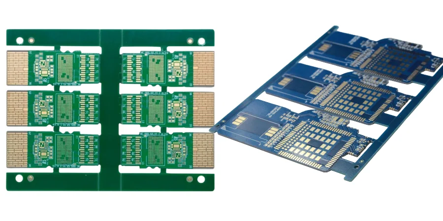
Potting/encapsulation: optical-electrical co-design and thermal power challenges in data center optical module PCBs
As data centers rapidly move into the 800G and even 1.6T era, optical modules—the heart of the network—face unprecedented PCB design and manufacturing challenges. As an engineer focused on TEC control and thermal management, I know that achieving tight optical, electrical, thermal, and mechanical coordination inside a tiny MSA form factor requires more than good routing and assembly. In this context, Potting/encapsulation is far more than a physical protection step: it is a core engineering decision that directly shapes thermal performance, signal integrity, and long-term reliability. From precise SMT assembly through final validation, every step is tightly coupled to the encapsulation strategy, and a single oversight can lead to catastrophic failures. This article explains the role of Potting/encapsulation across the full optical-module PCB lifecycle and how it balances high-speed signals, thermal power, and mechanical stress.
The real value of Potting/encapsulation: thermal–electrical co-optimization beyond “protection”
Traditionally, Potting/encapsulation is viewed as mechanical support plus moisture/vibration resistance. In modern high-speed optical modules, its role expands dramatically. The encapsulant becomes part of the thermal path and the EM environment; material choice and process details can make or break the module.
From a thermal perspective, the compound (typically epoxy, silicone, or polyurethane) must provide high thermal conductivity to carry heat from the laser (LD), driver IC, and DSP to the module housing. A common pitfall is focusing only on thermal conductivity (k) while ignoring cure shrinkage and CTE. If the encapsulant CTE mismatches the PCB laminate, chips, or optical components (TOSA/ROSA), temperature rise during operation or environmental thermal cycling creates significant mechanical stress—enough to crack solder joints, shift optical alignment, or even fracture chip substrates.
At HILPCB, we treat encapsulation material as an active “functional component” from the design stage. Based on power density, internal layout, and target operating temperature range, we select materials with strong CTE compatibility and excellent thermal performance. This ensures SMT assembly is not followed by an encapsulation step that introduces new failure mechanisms, but rather one that strengthens structural stability and thermal behavior.
Potting/encapsulation under MSA constraints: design and thermal management
MSA form factors such as QSFP-DD and OSFP impose strict dimensional limits. In such a small volume, PCB placement, component stacking, and thermal design must be pushed to the limit. Applying Potting/encapsulation becomes a millimeter-level precision operation: potting regions, material volume, and flow control during curing directly affect yield.
Thermal management is the biggest challenge here. Heat must be extracted along a carefully designed path: chip → TIM1 → substrate → TIM2/encapsulant → module housing → heatsink. In this path, the encapsulant effectively acts as TIM2. If bubbles or voids form during potting, their poor thermal conductivity creates local hot spots—raising junction temperature, degrading performance, and shortening lifetime.
To address this, Vacuum Potting has become a standard process for high-end modules. By dispensing and curing under vacuum, trapped bubbles are minimized and the thermal path becomes consistent and complete. During NPI EVT/DVT/PVT, we use thermal imaging and Finite Element Analysis (FEA) to simulate and validate potting effectiveness. Through iterative optimization early in NPI EVT/DVT/PVT, we can ensure that even under a harsh 85°C case condition, junction temperatures of critical devices remain within safe limits.
Chart: thermal performance comparison of common encapsulation materials
| Material type | Thermal conductivity (W/m·K) | CTE (ppm/°C) | Typical use case |
|---|---|---|---|
| Thermally conductive epoxy | 1.5 - 5.0 | 25 - 50 | High-power DSP and driver IC encapsulation |
| Thermally conductive silicone | 0.8 - 3.0 | 150 - 300 (flexible) | Stress buffering for optical components (TOSA/ROSA) |
| Low-Dk polyurethane | 0.5 - 1.2 | 60 - 100 | Localized potting near high-frequency signal regions |
How to read it: Material selection is always a trade-off. High-thermal epoxy often comes with higher CTE and fits chip hot zones; flexible silicone better protects fragile optics, sacrificing some thermal performance to relieve stress.
Signal integrity challenges: dielectric properties of Potting/encapsulation materials
As per-lane rates rise to 112G PAM4 and even 224G, Signal Integrity (SI) becomes a central design concern. Any material around PCB traces changes impedance and insertion loss. Potting/encapsulation materials are no exception: dielectric constant (Dk) and dissipation factor (Df) directly affect microstrip/stripline impedance and add extra insertion loss.
For potting areas near high-speed differential pairs, specialized low-Dk/low-Df compounds are required. Poor material choice causes impedance mismatch, reflections, and eye closure, pushing Bit Error Rate (BER) out of spec. In design, we use 3D EM simulation and include encapsulant dielectric properties in the model to predict impact on high-speed channels. This demands tight coupling between PCB design and manufacturing—for example, selecting high-speed PCB laminates from HILPCB to secure channel quality at the material level.
In production, Flying probe test is commonly performed before potting to catch latent opens/shorts, because once potting is complete, rework is close to impossible. Full electrical verification before encapsulation is therefore critical to final yield.
Deep integration of manufacturing and assembly: from SMT to encapsulation
Potting/encapsulation is not an isolated step; it is deeply coupled to the entire manufacturing flow. A successful encapsulation strategy starts in PCB design, runs through SMT assembly, and is protected by rigorous inspection.
A typical flow:
- SMT Assembly: All SMT components are precisely soldered onto the PCB.
- Inspection and verification: Use SPI/AOI/X-Ray inspection to check solder-joint quality. For BGA and other bottom-terminated devices, X-Ray is essential to detect hidden defects such as weak joints, bridging, or voids.
- Cleaning: Before potting, thoroughly clean the PCBA to remove flux residues and contaminants that can reduce adhesion.
- Localized potting/encapsulation: Use high-precision dispensing to inject a controlled volume into defined areas.
- Curing: Cure in an oven with tightly controlled temperature and time.
- Final assembly and inspection: In some designs, through-hole connectors or structural parts must be installed after potting. Here Selective wave soldering can precisely solder specific pins without affecting the cured potting region.
Across the process, SPI/AOI/X-Ray inspection provides critical process-control data. X-Ray not only validates BGA soldering, but can also be used after potting to detect internal voids, providing direct feedback for process optimization. HILPCB integrates capabilities from SMT assembly to complex encapsulation and inspection, ensuring seamless handoffs between steps.
HILPCB manufacturing capability: precision encapsulation and inspection
- Precision dispensing systems: Microliter-level dispensing accuracy and support for complex 3D profiles to keep material volume consistent.
- Vacuum potting equipment: Controls void rate to an industry-leading level (<1%), significantly improving thermal performance and reliability.
- In-line 3D X-Ray inspection: Used not only for BGA analysis, but also for non-destructive tomography of potted assemblies to pinpoint internal defects.
- Integrated process control: Unifies SMT, cleaning, potting, curing, and final test under one MES system to achieve end-to-end Traceability.
CMIS / management interface reliability and Potting/encapsulation
Modern optical modules are “smart” via management interfaces such as I2C/MDIO and the Common Management Interface Specification (CMIS). Through these interfaces, the host reads detailed module data (temperature, power, Tx/Rx optical power), performs diagnostics, and applies configuration. These functions rely on on-board EEPROM and MCU.
Potting/encapsulation must be handled carefully around these sensitive areas. Encapsulant flow and cure shrinkage can apply stress to fine-pitch EEPROM/MCU leads and cause connection failures. In addition, the chemistry must not corrode device packages.
Traceability is another key consideration. Each module’s unique serial number, calibration data, and supplier information are stored in EEPROM. This data must be programmed before potting at a dedicated programming station. After potting, the EEPROM is permanently sealed. Therefore, the final pre-potting step typically includes Flying probe test or a functional check to confirm I2C/MDIO communication and validate that EEPROM data was written correctly. This “last confirmation” is essential to avoid sealing defective semi-finished units inside the module.
Verification and test in NPI: ensuring post-potting performance consistency
A reliable Potting/encapsulation solution is not achieved in one shot—it must be refined and validated through strict NPI EVT/DVT/PVT (Engineering/Design/Production Validation Test) processes.
- EVT: Focus on material selection and baseline process validation. Build small engineering lots and run initial thermal cycling plus high/low temperature storage tests to evaluate CTE matching and adhesion. In this stage, use SPI/AOI/X-Ray inspection to assess soldering and encapsulation quality under early process conditions.
- DVT: The most demanding phase. Run full reliability tests on potted modules, including HAST, vibration/shock, and thousands of temperature cycles (-40°C to 85°C). The goal is to expose all latent design weaknesses, especially long-term potting-related failure modes such as delamination, cracking, or stress-driven performance drift.
- PVT: After design freeze, verify production readiness. Run pilot builds and monitor key parameters (dispense volume, cure profile) and process capability (Cpk), ensuring highly consistent encapsulation quality across units.
Across NPI EVT/DVT/PVT, HILPCB’s prototype assembly supports fast iteration, helping customers validate designs quickly and accelerate time-to-market.
Assembly advantage: end-to-end reliability assurance
At HILPCB, we don’t simply execute potting—we deliver a complete reliability solution. Our engineering team works with customers from the early project phase to define the encapsulation strategy. We use advanced simulation to predict thermo-mechanical stress distribution, validate the design via strict NPI processes, and monitor every detail with comprehensive inspection equipment. From PCB material selection to final functional testing, we ensure Potting/encapsulation strengthens performance instead of introducing risk.
Compatibility and long-term reliability: the final proof of encapsulation
The ultimate value of an optical module is its Compatibility across host systems and its ability to run stably over years. A carefully designed and validated Potting/encapsulation strategy is foundational.
It helps ensure that performance does not drift over time in complex data center EMI and thermal environments. For example, good encapsulation can reduce coupling between internal high-frequency circuits and external noise, preserving signal quality. It also prevents performance fluctuation driven by humidity swings or micro-vibration.
In some designs, even after main potting is complete, large through-hole parts such as power connectors must still be installed. In such cases, the precise thermal control of Selective wave soldering becomes critical. Local high temperature during soldering must not introduce secondary stress or damage in nearby potted regions, which requires careful profiling and masking-tool design. Ultimately, controlling these process details builds long-term reliability—keeping performance stable across a 5–7 year lifecycle. Choosing an appropriate high-thermal PCB material is the first step toward that goal.
Conclusion
In modern data center optical module development, Potting/encapsulation has long surpassed the concept of simple “physical protection”. It is an interdisciplinary engineering topic spanning materials science, thermodynamics, electromagnetics, and precision manufacturing. As a thermal power engineer, I believe only by treating encapsulation as a core design pillar—on par with chip selection and PCB layout—can teams truly manage optical-electrical coordination and thermal-power challenges.
From rigorous validation in NPI EVT/DVT/PVT, to seamless integration with SMT assembly, to comprehensive use of SPI/AOI/X-Ray inspection and other advanced methods, each step builds the foundation of final encapsulation quality. For equipment makers competing in a fierce market, a partner like HILPCB that provides one-stop service from design support through high-volume manufacturing is indispensable. A successful Potting/encapsulation strategy ultimately translates into better performance, longer lifetime, and higher customer trust.
Common Questions
Why is potting or encapsulation more than simple physical protection in optical modules?
Because it also influences EMI behavior, thermal paths, mechanical stress, and long-term signal stability. In dense optical hardware, encapsulation becomes part of the performance design rather than an afterthought.
What long-term reliability issues does encapsulation need to address?
It needs to control moisture effects, vibration response, stress on delicate parts, and performance drift over years of operation. Material choice and process quality both affect whether the module stays stable across its lifecycle.
Why do post-potting processes like selective wave soldering still matter?
Because some connectors or through-hole components may be installed after the main encapsulation step. Local heat and tooling must be controlled carefully so the existing potted areas are not damaged or overstressed.
What should teams validate before locking encapsulation for volume production?
They should validate compatibility, thermal performance, process repeatability, and long-duration reliability under realistic system conditions. That evidence is what turns a material choice into a production-ready strategy.