
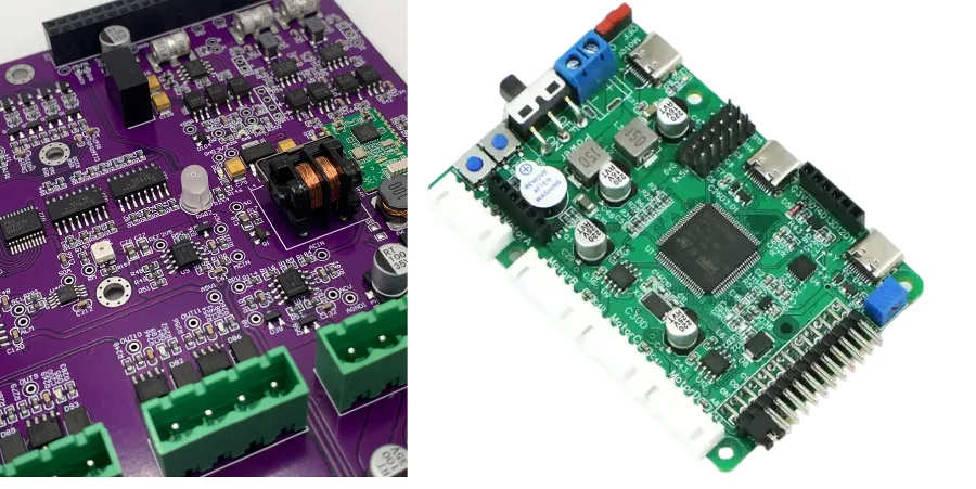
In modern industrial automation—especially in robotics—PROFINET has become the preferred communication protocol for motion control systems thanks to its excellent real-time performance and robust networking capabilities. Turning that protocol into stable, reliable physical hardware is a demanding engineering task. A successful PROFINET control PCB design is not just “connecting circuits”; it is a complex systems project that combines high-speed digital communication, high-power servo drives, precision analog feedback, and stringent safety requirements. From a motion-control engineer’s perspective, this article breaks down the key design elements of industrial robot control PCBs so your design can deliver deterministic real-time response and uncompromising operational safety in harsh industrial environments.
Servo drive loop: PWM, dead-time, and current-sense consistency
The servo drive loop is the heart of an industrial robot control board. Its performance directly determines motor response speed, positioning accuracy, and smooth operation. At the PCB level, handling PWM (Pulse Width Modulation) signals, dead-time, and current sensing is the top priority.
PWM and gate-drive layout
High-frequency PWM (typically 20 kHz to 100 kHz) drives power semiconductors (IGBT or MOSFET) to control the voltage and current delivered to motor windings. The rising and falling edges are steep and generate large dV/dt, making them a primary EMI source.
- Minimize loop area: The path from the gate driver to the power device gate—and the return path from the source/emitter back to the driver—forms the gate-drive loop. Likewise, the power-stage main loop (DC bus → power device → motor winding) must be minimized. Reducing these high-frequency current loop areas lowers parasitic inductance, suppresses overshoot and ringing, and reduces radiated EMI.
- Component placement: Place the gate-driver IC as close as possible to the power devices. In placement, prioritize the length and directness of these critical paths. For high-power applications, using heavy copper PCBs helps reduce impedance and temperature rise on power paths.
Dead-time control and consistency
To prevent shoot-through (both high-side and low-side devices conducting simultaneously), dead-time must be inserted into PWM. Too much dead-time distorts the output waveform and degrades control accuracy; too little increases shoot-through risk. Layout consistency is essential to keep dead-time precise and controllable across phases. Symmetrical placement and matched-length gate-drive traces help equalize signal delay and enable accurate dead-time control.
High-accuracy current sensing
Current sensing is the foundation for advanced motor-control algorithms such as FOC (Field-Oriented Control). Common methods include low-side shunt sensing and Hall-effect sensors.
- Shunt sensing: Cost-effective, but highly sensitive to PCB layout. Use Kelvin connections (separate current path and voltage-sense path) to eliminate errors from lead and solder-joint resistance. Route the sense traces as a differential pair, keep them away from noisy sources such as PWM switching nodes, and provide solid shielding with a ground plane. Accurate PROFINET control PCB impedance control is especially important for these sensitive analog signals.
Encoder/resolver interfaces: RS-485, EnDat, and BiSS-C layout essentials
Accurate position and speed feedback is the cornerstone of closed-loop motion control. Modern servo systems widely use high-speed serial absolute encoders such as EnDat and BiSS-C, which impose strict signal-integrity requirements.
Differential impedance and timing control
Whether it’s traditional RS-485 or high-speed EnDat 2.2 / BiSS-C, the physical layer is typically differential to improve common-mode noise immunity.
- Impedance control: Differential routing requires strict impedance control (typically 100 Ω or 120 Ω). A well-designed PROFINET control PCB stackup is the basis for achieving target impedance. Use professional impedance tools to determine trace width, spacing, and distance to reference planes. Discontinuities cause reflections, damage the eye diagram, and lead to communication errors.
- Length matching and symmetry: The two traces in a differential pair (P/N) must be tightly length-matched to avoid skew that converts to common-mode noise. Keep routing parallel and avoid sharp corners.
- Clock/data alignment: For synchronous protocols like EnDat and BiSS-C, clock-to-data timing is critical. Route related clock and data differential pairs as a group and control intra-group length differences within the allowable range.
Shielding and termination
- Termination: Place a termination resistor at the far end of the differential bus that matches the cable’s characteristic impedance to absorb energy and prevent reflections.
- Shield grounding: Ground the encoder cable shield at the PCB end with a single-point connection—often via an RC network or directly to chassis ground (FGND)—to provide low- and high-frequency shielding while avoiding ground loops.
Encoder interface PCB design comparison
| Feature | RS-485 (incremental) | EnDat 2.2 (absolute) | BiSS-C (absolute) |
|---|---|---|---|
| Data rate | Typically < 10 Mbps | Up to 16 MHz clock | Up to 10 MHz clock |
| Topology | Multi-drop bus | Point-to-point | Point-to-point or multi-slave bus |
| Key PCB layout considerations | Differential impedance control, bus termination, avoid stubs. | Strict differential impedance plus clock/data pair length matching; low-capacitance design. | Strict differential impedance control; clock/data pair length matching; supports daisy-chain layout. |
| Use cases | Simple, low-cost position feedback. | High-performance, high-safety servo applications. | High-performance, open-standard servo applications. |
Digital isolation and common-mode suppression: reliable design in high dV/dt environments
In motor drives, there is a large potential difference and severe common-mode transients (CMTI) between the control side (MCU, FPGA) and the power side (IGBT/MOSFET bridge). Effective electrical isolation is the lifeline for system safety and signal integrity.
- Creepage and clearance: PCB layout must comply with safety standards (e.g., IEC 61800-5-1) for creepage and clearance. This means sufficient physical spacing on both outer and inner layers across the isolation boundary. Creating a copper keep-out area under the boundary is standard practice.
- Digital isolator selection: Compared with optocouplers, modern capacitive or magnetic digital isolators provide higher speed, lower power, longer life, and much stronger CMTI. Choose isolators with high CMTI ratings (>100 kV/μs) to suppress high dV/dt noise from motor switching.
- Isolated power: The secondary side (power side) needs an independent isolated supply, typically via an isolated DC/DC converter. Its layout must follow the same isolation rules, and the PCB area under the transformer should be kept copper-free.
- Common-mode chokes: Proper use of common-mode chokes on PROFINET, encoder interfaces, and power inputs helps filter common-mode noise and improves immunity.
A robust PROFINET control PCB validation flow must include Hipot testing to verify isolation barrier integrity and dielectric withstand.
Braking unit and energy dissipation: balancing safety and thermal design
When a robot arm decelerates or lowers a load, the motor operates as a generator and returns regenerative energy to the DC bus, increasing bus voltage. The braking unit connects an external braking resistor when the bus exceeds a threshold, dissipating excess energy as heat.
Thermal management design
- Braking resistor placement: The braking resistor is a primary heat source; placement is critical. Keep it away from temperature-sensitive components (electrolytic capacitors, precision op-amps, MCU), and ideally near the PCB edge or an airflow opening.
- Copper pour and thermal vias: Use large copper areas under and around the resistor as a heat spreader, and transfer heat to other layers or a backside heatsink with dense thermal vias. This is essential for consistent thermal performance from PROFINET control PCB low volume prototypes to PROFINET control PCB mass production.
High-current paths and safety integration
- Braking chopper: The power switch (typically IGBT or MOSFET) that connects/disconnects the braking resistor—and its gate drive—should follow similar rules to the main inverter: minimize the power loop to handle fast high-current switching.
- Safety functions (E-Stop): The braking circuit is often tightly integrated with safety functions such as E-Stop. When a safety shutdown triggers, forced braking may be required to achieve fast, controlled stopping. Routing for relays, drives, and feedback signals must be reliable and well isolated from other circuits.
Key braking and safety design points
- Prioritize thermal management: Keep high-power braking resistors away from sensitive parts, and use large copper areas and thermal vias for efficient heat spreading.
- Optimize high-current paths: Keep braking-chopper routing short and wide to minimize parasitic inductance/resistance, reduce switching loss, and limit voltage spikes.
- Ensure safety-circuit integrity: Route E-Stop and safety-relay signals clearly and directly, and physically isolate them from noisy power circuits to guarantee reliable triggering under all conditions.
- Consider component lifetime: Frequent braking causes thermal cycling; select high-reliability power devices and resistors and apply sufficient derating during design.
Immunity design: ESD/EFT/surge and return-path control
Industrial environments are full of electromagnetic noise sources such as ESD, EFT, and surge. A robust PROFINET control PCB design must deliver strong EMC performance.
Grounding and return-path control
- A single, continuous ground plane: For mixed-signal systems that include high-speed digital, sensitive analog, and high-power switching, a single, continuous ground plane is best practice. It provides the lowest-impedance return path for signals. Split ground planes often cause more problems by forcing return currents to detour, forming large loop antennas that increase EMI and crosstalk.
- Return-path awareness: Always think about the return path during layout. Return current for high-speed signals follows the path directly beneath the trace on the adjacent reference plane. Routing across split regions is a major EMC anti-pattern. An optimized PROFINET control PCB stackup—for example, sandwiching high-speed signal layers between two ground planes (stripline)—provides the best shielding and return-path control.
Interface protection
- TVS diodes: Place TVS diodes close to the connector on all external interfaces (PROFINET, encoders, I/O) to provide a discharge path for ESD/EFT and other transient overvoltage events.
- Filter networks: Use π or T filter networks (capacitors plus ferrite beads) to filter conducted noise entering or leaving the PCB.
Working with an experienced manufacturer like HILPCB helps ensure your design is correctly implemented in production—whether for fast-iteration prototype assembly or volume manufacturing. Their expertise is critical for complex PROFINET control PCB impedance control and stackup execution.
Common Questions
Why do PWM loops and current-sense traces need careful layout on servo control boards?
Because fast switching edges create high dV/dt, overshoot, and EMI, while current-sense signals are small and noise-sensitive. Short loops, close gate-driver placement, and Kelvin or differential sensing improve control accuracy and stability.
Why are impedance and timing control important on encoder and resolver interfaces?
Protocols such as RS-485, EnDat, and BiSS-C depend on clean differential signaling. Poor impedance control, skew, or clock/data mismatch can distort the eye diagram and create position-feedback errors.
Why are digital isolation and isolated power essential in robot control PCBs?
They separate the low-voltage control domain from the noisy power stage and protect both safety and signal integrity. High-CMTI isolators, proper creepage and clearance, and isolated power rails help the system survive harsh switching transients.
Why are continuous ground planes and return-path control so important for EMC?
Return current follows the reference plane beneath the signal. Continuous planes minimize loop area and noise coupling, while split planes often force detours that increase EMI and reduce immunity.
Conclusion
A successful PROFINET control PCB design is an art of balancing performance, cost, reliability, and safety. Engineers must understand not only schematics, but also how high-frequency signals, high-current switching, and sensitive analog networks behave on a real PCB. From servo power-loop placement to encoder-interface signal integrity, and from isolation and thermal management to EMC strategy, every detail affects the final outcome.
Whether you are building PROFINET control PCB low volume prototypes for proof-of-concept or scaling to PROFINET control PCB mass production, following the principles discussed here—and partnering with capable specialists such as HILPCB with high-speed PCB manufacturing strength—will help you deliver stable, efficient, and safe industrial robot control systems. Ultimately, excellent PROFINET control PCB design gives your robots precise motion capability and rock-solid reliability.