
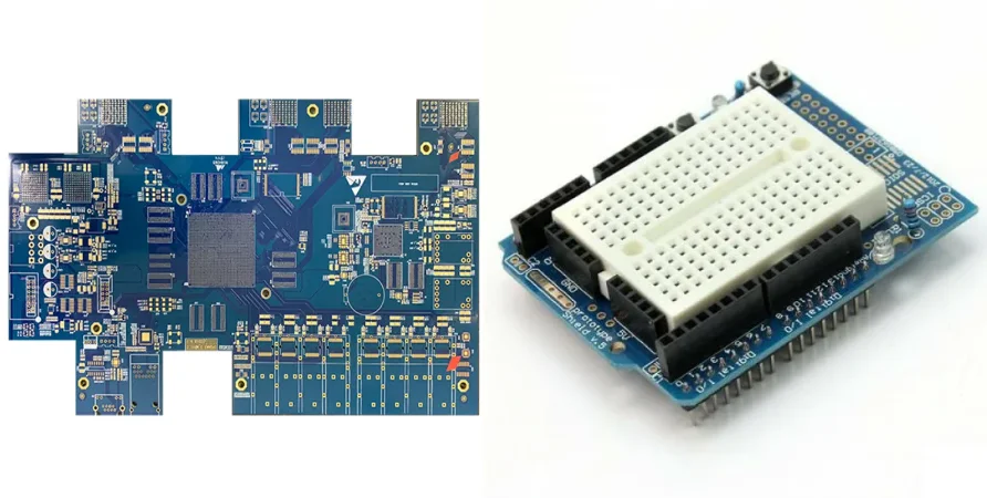
Prototype PCB manufacturing is not only about receiving a board quickly. For engineering teams, the real goal is to get a build that answers the right design question: does the circuit work, can the stackup be manufactured, will the impedance plan survive fabrication, and what must be changed before pilot production?
A useful prototype PCB process should therefore balance speed with engineering control. Fast delivery matters, but it should not come at the cost of unclear stackups, unverified drill rules, untested nets, or undocumented material substitutions. This is especially important for HDI prototypes, rigid-flex prototypes, RF boards, power electronics, medical electronics, industrial controls and other designs where the first build is meant to reduce risk rather than simply prove that Gerber files can be fabricated.
This guide explains how HILPCB approaches quick-turn prototype PCB manufacturing for R&D teams: DFM review, material selection, stackup planning, controlled impedance, electrical testing, prototype PCBA, small-batch iteration and RFQ handoff.
Key takeaways
- A quick-turn prototype is valuable only when it is built around a clear engineering objective: electrical bring-up, mechanical fit, thermal validation, firmware testing, RF tuning, or production-risk reduction.
- DFM review should happen before fabrication starts, especially for HDI, rigid-flex, controlled-impedance, heavy-copper, high-frequency and mixed-material builds.
- Prototype boards should use materials, copper weights, stackups and surface finishes that are close enough to the intended product to make test results meaningful.
- Bare-board electrical testing, impedance coupon testing and PCBA inspection should be defined in the RFQ rather than added after the board is already built.
- A prototype supplier should help the team move from first build to pilot lot by keeping stackup records, material lots, impedance data, inspection results and assembly feedback traceable.
In this guide
- What a prototype PCB should prove
- Quick-turn does not mean skipping DFM
- Choosing the right prototype route
- Stackup, materials and impedance planning
- Prototype PCBA, inspection and test
- Common prototype PCB failure modes
- Cost drivers and RFQ checklist
- Reference standards and review boundaries
- FAQ
What a prototype PCB should prove
A prototype PCB should not be treated as a miniature version of mass production by default. Its job depends on the stage of the hardware program.
For an early concept build, the goal may be to confirm basic circuit function, connector placement, mechanical fit and firmware bring-up. For a second or third engineering build, the goal may shift toward controlled impedance, thermal behavior, power integrity, RF performance or manufacturability. For a pilot build, the prototype should start looking like a production-intent board, with a stable stackup, defined test plan, documented material choices and repeatable assembly process.
The first question in every prototype request should be simple: what decision should this build help you make?
| Prototype objective | What the PCB must support | What to avoid |
|---|---|---|
| Circuit bring-up | Fast fabrication, accessible test points, enough soldering margin for rework | Over-optimizing cost before the circuit is proven |
| Mechanical fit | Correct outline, mounting holes, connector placement, thickness and bend zones | Changing board thickness or connector footprints after enclosure checks |
| RF or high-speed validation | Stable stackup, controlled impedance, smooth copper options, impedance coupons and launch consistency | Treating a substitute material as electrically equivalent without review |
| Power and thermal validation | Correct copper weight, current paths, thermal vias, heavy copper or copper coin if required | Using thin prototype copper when production needs high-current structure |
| Rigid-flex validation | Realistic bend radius, stiffener, coverlay and adhesive stackup | Replacing flex with cable in prototype and assuming the same reliability |
| Pilot / pre-production | Test coverage, traceability, panelization, assembly fixtures and documentation | Building a beautiful prototype that cannot be repeated at volume |
This distinction protects the team from a common mistake: ordering the fastest possible board, then trying to use it as proof for reliability, thermal margin or production readiness. A fast prototype can support those questions only if the release package was planned for them.
Quick-turn does not mean skipping DFM
Speed and DFM are not opposites. In prototype work, DFM is often what keeps the build fast because it catches problems before they become CAM holds, fabrication delays or failed first articles.
A good prototype PCB fabrication review should check more than trace width and spacing. It should confirm whether the board can be manufactured with the requested layer count, copper weight, drill structure, solder mask registration, surface finish, impedance target and assembly requirements.
Key DFM checks include:
- Board outline and mechanical data: route path, cutouts, slots, castellations, edge plating and tolerances.
- Stackup consistency: layer count, dielectric thickness, copper weight, resin content and material availability.
- Drill structure: mechanical drill limits, laser via aspect ratio, buried/blind via feasibility, via fill and via-in-pad rules.
- Copper balance: large copper pours, heavy copper transitions, thermal reliefs and risk of bow or twist.
- Solder mask and silkscreen: fine-pitch pads, mask dams, exposed copper, component markings and polarity marks.
- Surface finish choice: ENIG, immersion silver, OSP, HASL or ENEPIG based on pitch, shelf life, wire bonding or multiple reflow cycles.
- Test access: bare-board netlist, impedance coupons, ICT pads, programming headers and functional test points.
- Assembly risk: BGA pitch, QFN thermal pads, stencil design, component clearance and rework access.
For simple two-layer boards, many of these checks are quick. For HDI, rigid-flex, RF, high-current or high-voltage prototypes, they are essential. A design that is technically correct in CAD can still be difficult to build if the drill stack, copper distribution, bend region, or material substitution is not discussed before fabrication.
Choosing the right prototype route
Not every prototype belongs on the same manufacturing path. The best route depends on what the team needs to learn.
Standard rigid prototype PCB
A standard rigid prototype is best for early circuit validation, firmware bring-up, connector testing, simple power boards and low-to-moderate density digital hardware. These builds usually prioritize turnaround time, clean fabrication, readable documentation and flexible quantity.
The team should still define copper weight, finish, board thickness, electrical test requirements and panelization expectations. Even a simple board can fail schedule if the mechanical drawing, stackup, or solder mask requirement is ambiguous.
HDI prototype PCB
An HDI PCB prototype is appropriate when the design uses fine-pitch BGAs, dense processors, camera modules, compact RF front ends, wearable electronics or miniaturized IoT hardware. HDI introduces laser microvias, buried vias, stacked vias, staggered vias, via-in-pad, resin filling and additional lamination steps.
HDI prototypes should be reviewed early because small changes in via structure can affect cost, yield, reliability and lead time. If the final product is expected to use HDI, the prototype should not hide that risk by using a larger temporary package unless the team clearly understands the tradeoff.
Rigid-flex prototype PCB
A rigid-flex PCB prototype is useful when the board must fold into an enclosure, replace a cable harness, reduce connector count, or survive motion and vibration. It is common in wearables, medical electronics, drones, cameras, handheld devices and compact industrial modules.
Rigid-flex prototypes need a more complete mechanical discussion than rigid boards. Bend radius, flex length, dynamic versus static flexing, stiffener thickness, adhesive or adhesiveless polyimide, coverlay openings and assembly forming all affect the result. A board that works flat on a bench may fail once it is folded into the product.
High-frequency and RF prototype PCB
RF prototypes require more than a controlled impedance note. The material, copper foil roughness, laminate thickness, solder mask over RF traces, connector launch, via fence, ground stitching and test coupon structure can all change the measurement.
For antennas, radar, 5G modules, microwave circuits and high-speed interconnect, the prototype should be built with a material and stackup close to the intended design. If a substitute material is used to save time, test conclusions should be limited to bring-up, not final RF behavior.
Power and high-current prototype PCB
Power prototypes need current-carrying structure, thermal path and spacing review. Heavy copper, busbar-style pours, thermal vias, copper coins, high-Tg material, creepage and clearance, slotting and high-current terminals should be discussed before the first build.
For motor drives, LED drivers, battery systems, inverters and power modules, a low-cost prototype with thinner copper may bring up the control circuit but will not prove real thermal or current performance.
Stackup, materials and impedance planning
The stackup is one of the most important decisions in prototype PCB manufacturing. It defines reference planes, impedance behavior, power distribution, mechanical thickness, lamination yield, cost and lead time.
For simple boards, a standard stackup may be enough. For high-speed, RF, power, HDI or rigid-flex work, the stackup should be reviewed before final routing. Moving dielectric thickness or reference layers after routing can change impedance, length matching, via behavior and return paths.
| Design type | Stackup priority | Prototype review focus |
|---|---|---|
| MCU / IoT board | Cost, manufacturability, test access | Stable 2–6 layer stackup, clear power/ground return paths |
| High-speed digital board | Reference planes, impedance and via transitions | Differential pairs, via stubs, return continuity, impedance coupons |
| RF board | Material Dk/Df, copper roughness and launch geometry | RF connector launch, solder mask, via fence, ground continuity |
| Power board | Copper thickness, heat spreading and spacing | Current density, thermal vias, creepage/clearance, connector strength |
| HDI board | Via architecture and lamination sequence | Microvia reliability, via-in-pad, BGA escape, resin fill |
| Rigid-flex board | Bend reliability and rigid-flex transition | Bend radius, coverlay, stiffeners, dynamic flex limits |
Material selection
Prototype material should be selected based on what the build needs to prove. FR-4 is appropriate for many digital and control boards, but high-frequency, low-loss, high-temperature, high-voltage or high-current designs may need more specific laminates.
Common material questions include:
- Is the prototype only checking logic function, or does it need real RF/high-speed behavior?
- Does the board need high-Tg material for lead-free assembly, thermal cycling, or power density?
- Are controlled impedance and loss budget important enough to require a named laminate?
- Is the final product expected to use Rogers, PTFE, LCP, ceramic, metal-core or hybrid construction?
- Will the prototype go through multiple reflow cycles or rework?
Controlled impedance
Controlled impedance is not created by writing “50 ohm” or “100 ohm differential” in a note. It depends on trace geometry, copper thickness, dielectric thickness, Dk, solder mask and fabrication tolerance.
For prototype builds, the RFQ should state:
- target impedance and tolerance
- single-ended or differential structure
- layers and reference planes
- coupon requirements
- whether TDR reporting is required
- whether the manufacturer may adjust trace width to meet the stackup
Using an impedance calculator is useful during planning, but the final values should be aligned with the actual manufacturing stackup.
Prototype PCBA, inspection and test
Many prototype failures appear only after assembly. A board can pass bare-board electrical test and still fail if the footprint, stencil, component orientation, thermal pad, BGA escape, or power-up sequence was not planned.
HILPCB supports prototype PCBA through SMT assembly, through-hole assembly, component procurement, solder paste printing, reflow, selective soldering, manual operations where needed, inspection and functional test support.
Prototype assembly review
Before assembly, the package should include more than Gerbers:
- BOM with manufacturer part numbers, alternates and DNP items
- centroid / pick-and-place file
- assembly drawing with polarity and connector orientation
- stencil notes for QFN, BGA, fine-pitch and thermal pads
- special handling notes for moisture-sensitive, ESD-sensitive or expensive parts
- programming, boot mode and test fixture requirements
- acceptance criteria for inspection and rework
Inspection methods
| Inspection or test method | What it can catch | Where it is most useful |
|---|---|---|
| AOI | Missing parts, polarity errors, skew, visible solder defects | SMT prototype assembly |
| X-ray | BGA/QFN hidden joints, bridges, voiding, via-in-pad solder issues | Dense boards and bottom-terminated components |
| Bare-board electrical test | Shorts and opens before assembly | All prototype fabrication, especially multilayer boards |
| Flying probe | Flexible electrical test without expensive fixtures | Prototypes and low-volume builds |
| ICT | Component-level test through fixture access | Pilot and repeat builds with stable design |
| Functional test | Product-level operation under defined conditions | Firmware bring-up, power boards, communication modules |
| TDR / impedance test | Impedance consistency and coupon behavior | High-speed and RF prototypes |
| Hi-Pot / insulation resistance | Isolation behavior under defined test conditions | High-voltage and safety-related boards |
Testing should be matched to the prototype objective. A simple bring-up build may need only bare-board electrical test and visual inspection. A pilot build may require impedance reports, X-ray images, programming logs, functional test data and material traceability.
Common prototype PCB failure modes
Prototype problems are often not caused by one dramatic mistake. They come from small mismatches between design intent, fabrication assumptions and assembly reality.
| Failure mode | Likely cause | Prevention |
|---|---|---|
| Board arrives late after CAM hold | Missing drill table, unclear stackup, invalid outline or ambiguous notes | Send complete Gerber/ODB++, drill files, drawing and stackup request |
| Impedance is different from simulation | Material substitution, changed dielectric thickness, solder mask effect or trace width adjustment | Approve production stackup before routing or allow width compensation |
| BGA does not assemble cleanly | Pad design, stencil opening, via-in-pad fill, warpage or moisture control issue | Review BGA footprint, via fill and stencil design before build |
| Rigid-flex cracks near transition | Bend radius too tight, missing strain relief, copper in bend area or wrong stiffener placement | Define bend radius, static/dynamic use and flex stackup early |
| RF prototype measures poorly | Connector launch, solder mask, via fence, copper roughness or test fixture issue | Include RF launch review, coupon design and measurement plan |
| Power board overheats | Prototype copper weight or thermal path does not match real load | Use production-intent copper and thermal structure for thermal validation |
| Assembly rework damages board | Fine-pitch layout, poor access, incompatible finish or thermal imbalance | Plan rework access, finish and thermal relief before PCBA |
| Test coverage is too low | No test points, inaccessible nets or missing programming interface | Include test access and fixture planning before layout freeze |
The best prototype process reduces unknowns in layers. It does not try to answer every question in one build. Instead, it defines what the current revision should prove, gathers data, updates the design, and moves the program toward a more production-ready release.
Cost drivers and RFQ checklist
Prototype PCB pricing depends on lead time, complexity, material, process risk and test requirements. The cheapest prototype is not always the lowest-cost engineering decision. A board that requires re-spin because the material, stackup or test plan was wrong can cost more than a slightly slower but better-controlled build.
Major cost drivers
- layer count and board size
- urgent lead time
- HDI lamination cycles
- blind, buried, stacked or filled vias
- controlled impedance and test coupons
- high-frequency or special material
- rigid-flex construction
- heavy copper, copper coin or metal core
- ENIG, ENEPIG or other premium finishes
- tight tolerance drilling, slotting or edge plating
- assembly complexity and component sourcing
- X-ray, functional testing, programming and reports
RFQ checklist for quick-turn prototype PCB
Send these files and requirements when requesting a quote:
- Gerber or ODB++ fabrication data
- NC drill files and drill map
- board outline drawing with dimensions and tolerances
- layer stackup request or target finished thickness
- copper weight by layer
- controlled impedance table, if required
- material preference or electrical requirements
- surface finish preference
- solder mask and silkscreen color
- panelization requirements, if any
- IPC class or acceptance requirement, if specified
- bare-board electrical test requirement
- impedance coupon and report requirement
- assembly BOM, centroid file and assembly drawing for PCBA
- programming, firmware, fixture and functional test instructions
- quantity, lead time target and shipping destination
For urgent revisions, clearly mark what changed from the previous version. This helps engineering and CAM review focus on the right risk areas instead of re-checking the entire design from scratch.
Reference standards and review boundaries
Prototype PCB manufacturing can use industry standards as acceptance and documentation references, but a prototype board does not automatically become product-certified because it was built or inspected against a standard.
- IPC-6012: Common reference for qualification and performance requirements of rigid printed boards.
- IPC-A-600: Common reference for externally and internally observable acceptability conditions on printed boards.
- IPC-9252: Common reference for electrical testing of unpopulated printed boards and innerlayers.
- IPC-A-610: Common reference for acceptability of electronic assemblies after PCBA.
- J-STD-001: Common reference for soldered electrical and electronic assemblies.
- Customer drawings and product requirements: Always take priority when they define tighter stackup, reliability, cleanliness, test or documentation requirements.
For regulated industries such as medical, automotive, aerospace, defense, energy or transportation, prototype boards support product development and verification, but final compliance still depends on the complete device, its risk file, validation plan, production process and applicable regulatory pathway.
Why work with HILPCB for prototype PCB manufacturing?
HILPCB supports quick-turn prototype PCB manufacturing for teams that need speed, but also need the prototype to be technically meaningful. We support simple rigid boards, HDI prototypes, controlled-impedance builds, rigid-flex prototypes, high-frequency materials, metal-core boards, heavy-copper designs and prototype PCBA.
Our engineering support can help review:
- stackup feasibility
- material substitution risk
- impedance and coupon planning
- HDI via structure
- rigid-flex bend and stiffener design
- solder mask and surface finish selection
- DFM/DFA issues before fabrication
- assembly and test access
- documentation needed for the next build
For teams moving from first prototype to pilot production, we can also help keep the build history clear: stackup records, material choices, impedance results, electrical test status, inspection images, assembly feedback and functional test notes.
Ready to build a prototype PCB?
Send your Gerber or ODB++ package, drill files, stackup notes, material requirements and quantity through the quote page. For a bare-board build with a defined prototype objective, use the prototype PCB service route; if the board also needs assembly, include the BOM, centroid file, assembly drawing and any programming or functional test requirements.
For the fastest review, include one sentence explaining the goal of the prototype: bring-up, RF validation, thermal test, enclosure fit, firmware development, pilot build, or production-risk reduction. That one sentence helps the manufacturing review focus on what matters most for your current hardware stage.
FAQ
What is the difference between a prototype PCB and a production PCB?
A prototype PCB is usually built to answer an engineering question quickly, while a production PCB is built for repeatability, cost control, documentation and long-term supply. Some prototypes are simple first-build boards, while others are production-intent pilot lots with controlled stackups, impedance reports, inspection data and functional testing.
How fast can a prototype PCB be manufactured?
Lead time depends on layer count, material, surface finish, HDI structure, rigid-flex construction, impedance control, assembly complexity and test requirements. Simple boards can usually move much faster than special-material, high-layer-count, HDI, heavy-copper or rigid-flex builds.
Should I use the same material in the prototype as in production?
Use the same or a closely equivalent material when the prototype is validating RF, high-speed, thermal, high-voltage or mechanical behavior. If the prototype is only for firmware bring-up or fit checking, a substitute material may be acceptable, but the test conclusions should be limited.
Do prototype PCBs need electrical testing?
Yes, bare-board electrical testing is strongly recommended because it catches shorts and opens before assembly. For high-speed or RF boards, impedance testing and coupons may also be needed. For high-voltage boards, insulation or Hi-Pot test requirements should be defined in the RFQ.
Can HILPCB assemble prototype PCBs too?
Yes. HILPCB can support prototype PCBA, including SMT, through-hole assembly, component sourcing, AOI, X-ray where needed, functional test support and programming instructions supplied by the customer.
What files should I send for a prototype PCB quote?
Send Gerber or ODB++, NC drill files, a board drawing, stackup notes, material requirements, copper weight, impedance table if applicable, surface finish, quantity and lead time target. For assembly, also send BOM, centroid file, assembly drawing and test/programming instructions.