
QFN assembly depends on both the perimeter terminals and the exposed center pad. Too much paste on the center pad can lift the package and contribute to open perimeter joints. Open vias can wick solder away from the joint and may contribute to voiding. Before layout release, define the perimeter lands for the actual terminal style, start the exposed-pad paste pattern from the component maker's guidance, and agree on the via construction with the fabricator and assembler.
The rest of this page works through those three decisions with numbers, then covers inspection, because QFN joints are mostly hidden and need a plan for evidence.
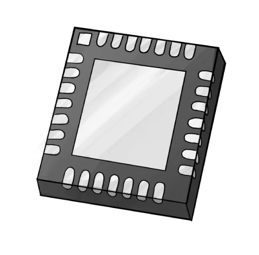
1. What Is Under a QFN, and Why It Changes the Footprint
A quad flat no-lead package has a die attached to a copper lead frame, molded in epoxy, with terminals exposed on the bottom along four edges and a large exposed pad (EP) in the center. The EP is the main heat path from the die into the board and is often the ground connection. Common body sizes run from 2 × 2 mm to 12 × 12 mm, at 0.4, 0.5 or 0.65 mm pitch, with seated heights from about 0.35 mm (ultra-thin) to 1.0 mm. Naming varies by supplier (QFN, DFN for two-sided parts, VQFN, WQFN, MLF), so the package outline drawing in the datasheet is the only reliable source for dimensions.
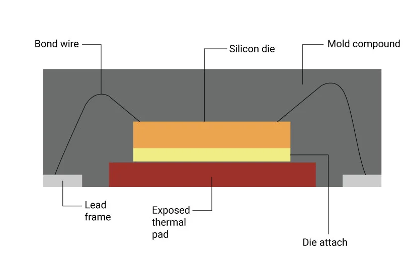
The terminal style decides what kind of solder joint you can get:
| Terminal style | Exposed copper on package side | Visible toe fillet after reflow | Inspection consequence |
|---|---|---|---|
| Sawn, fully exposed | The cut face may expose unplated copper | Partial or none, depending on the package and wetting | Limited optical evidence; X-ray may reveal some defects |
| Pull-back | Terminal stops short of the body edge | Generally not visible | The joint is largely hidden; optical coverage depends on the view |
| Side wettable flank (SWF) | A solderable flank is exposed at the side | Designed to form a visible fillet | AOI may inspect the accessible fillet, subject to the part and inspection setup |
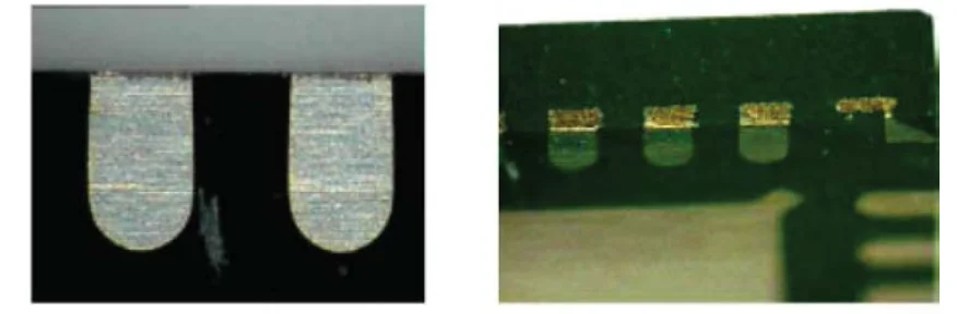
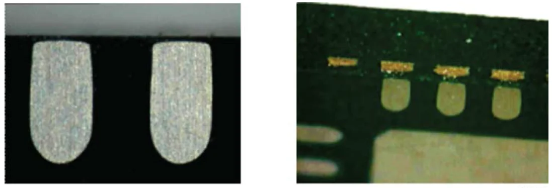
If the product needs optical evidence of side wetting, consider an SWF part during component selection and agree on the inspection criteria. A footprint change cannot expose a terminal that stops short of the package edge.
2. Perimeter Land Pattern: Start From the Package Drawing
Build the perimeter lands from the datasheet's recommended land pattern when one exists. If it does not, derive them from the package terminal dimensions using IPC-7351 principles (see our IPC-7351 land pattern guide):
- Toe extension: Use the package maker's recommended extension beyond the package edge. For SWF parts, check that the land supports the specified visible fillet; excessive extension may increase bridging risk.
- Heel extension: Extend inward modestly past the terminal end, keeping enough gap to the EP land that a solder mask web fits between them.
- Land width: Approximately the terminal width, often trimmed slightly at 0.4 mm pitch to protect the mask web between lands.
- Corner lands: Check for lands that wrap the corner or tie-bar features shown on the outline drawing; omitting them is a common library error.
Solder mask between lands
At 0.5 mm pitch with 0.25 mm wide lands, the copper gap is 0.25 mm. With a 0.05 mm mask expansion per side, the nominal mask web is 0.15 mm. At 0.4 mm pitch with 0.20 mm lands, the same expansion leaves a nominal 0.10 mm web. Actual capability depends on the fabricator, mask and tolerances. If the web cannot be held, discuss a gang (group) opening and the associated bridging controls with the fabricator and assembler. A partially formed web may leave mask slivers. Our solder mask design guide covers web, expansion and SMD/NSMD choices in more detail.
3. Exposed Pad Paste: Sizing the Windowpane
The EP land is often the same size as the package's exposed pad, or slightly smaller. A single full-size stencil aperture can deposit more solder than the joint needs. Excess solder may lift or tilt the package and contribute to perimeter opens; large deposits can also make volatile removal more difficult. Actual results depend on the package, paste, stencil and reflow process.
Component makers often specify smaller, separated apertures (a "windowpane") for a particular package. Start with the applicable part's recommended land and stencil pattern, including foil thickness, then qualify the print and reflow process. Aperture area coverage is a geometric ratio, not a measurement of printed paste volume or finished solder coverage.
Worked example: QFN-48, 7 × 7 mm body, 5.6 × 5.6 mm EP
EP land area = 5.6 × 5.6 = 31.4 mm². With a 0.12 mm stencil:
| Aperture pattern | Aperture size | Coverage | Notes |
|---|---|---|---|
| Single opening | 5.6 × 5.6 mm | 100% | May deposit excess paste; assess package float and voiding |
| 2 × 2 windowpane | 2.2 × 2.2 mm | 61.7% | Four separated deposits |
| 3 × 3 windowpane | 1.5 × 1.5 mm | 64.6% | Nine separated deposits |
| 3 × 3 windowpane | 1.6 × 1.6 mm | 73.5% | Greater aperture area; assess the printed volume and joints |
| 4 × 4 windowpane | 1.1 × 1.1 mm | 61.7% | Sixteen smaller deposits |
These are area comparisons, not qualified production patterns. Window spacing, via diameter, array pitch and relative placement must be designed together; no alignment with a via grid is implied.
Check the area ratio of each window, as you would for small apertures (see our SMT stencil design guide). A 1.1 mm square window in 0.12 mm foil has an area ratio of 1.1 / (4 × 0.12) = 2.3. A 0.25 × 0.7 mm perimeter aperture in the same foil has an area ratio near 0.77, making it a more demanding feature for paste release. Area ratio alone does not guarantee transfer: check the stencil maker's process limits and verify print volume and position with SPI.
4. Thermal Vias Under the Exposed Pad
The EP only works as a heat path if heat can get through the board. Thermal vias carry it to inner planes and the opposite side (see our thermal via design guide). A first-order estimate of one via's conduction resistance is:
A = (π / 4) × (D_outer² - D_inner²)
R_via = L / (k_Cu × A)
Here A is the copper barrel cross-sectional area, L its length, k_Cu the copper thermal conductivity, and D_inner = D_outer - 2t for uniform wall thickness t. Use consistent units. For an illustrative 1.6 mm barrel with a 0.30 mm copper barrel outer diameter, 25 µm uniform copper wall and k_Cu = 390 W/(m·K), A is approximately 0.0216 mm² and R_via approximately 190 °C/W. The barrel outer diameter is an assumed model dimension, not an unspecified drill diameter; determine the actual finished geometry with the fabricator.
| Via array | Approximate R through board | Comment |
|---|---|---|
| 5 identical vias | ~38 °C/W | Ideal parallel paths |
| 9 identical vias | ~21 °C/W | Ideal parallel paths |
| 16 identical vias | ~12 °C/W | Ideal parallel paths |
The model assumes one-dimensional conduction, isothermal ends and independent identical paths in parallel. It omits heat spreading, solder layers, voids and other heat paths. It cannot establish a junction temperature, the suitability of a power level or the relative effect of voids; validate the actual assembly with a suitable thermal model and, where needed, measurements.
Via treatment and assembly risks
| Via treatment | Solder wicking | Voiding tendency | Cost and notes |
|---|---|---|---|
| Open, untented | Solder may wick into the barrel or appear on the far side | Open barrels may contribute to voiding | Discuss hole size, aperture placement and process trials with the assembler |
| Tented from the bottom side | A sound tent may reduce flow through the far side | Entrapped gas and tent integrity still require evaluation | Confirm tent coverage and reliability with the fabricator |
| Plugged (non-conductive fill), unplated surface | May reduce wicking, depending on plug integrity | Depends on the construction and process | Specify fill and allowable surface recess or protrusion |
| Filled and capped (via-in-pad plated over, VIPPO) | A sound plated cap isolates the hole from the pad surface | Joint voiding can still occur from other causes | Specify fill, cap and surface quality. See our via-in-pad guide |
For open vias, placing stencil openings away from the holes may help limit direct paste deposition over them, but it does not guarantee that solder will not wick. Check the actual hole diameter, aperture spacing and manufacturing tolerances, then verify the result on an assembly trial. Our solder wicking guide discusses the mechanism.
5. QFN Defect Diagnostic Matrix
| Symptom | Evidence to pull | Possible causes to investigate | Checks or trials |
|---|---|---|---|
| Perimeter opens | Electrical test, X-ray views and package height or tilt | Excess EP paste, insufficient perimeter paste or placement and warpage | Compare SPI deposits and standoff with the qualified process; trial a revised aperture if warranted |
| High EP voiding | X-ray void map and reflow records | Paste, aperture pattern, moisture, vias or reflow conditions | Review each variable and qualify changes against the agreed criteria |
| Solder balls or bumps on the far side under the EP | Far-side visual inspection and via locations | Solder wicking through open or incompletely sealed vias | Check via construction and paste placement; trial a suitable treatment |
| Bridging between perimeter terminals | AOI or X-ray views, SPI data and bare-board mask inspection | Paste volume, placement, mask or land geometry | Verify the cause before adjusting stencil, mask or land geometry |
| Package skew or rotation | Placement AOI before reflow and post-reflow offset | Placement offset or uneven solder forces | Check placement data, deposits and package library |
| Intermittent joints after thermal cycling | Electrical failure data and cross-section of the failed joint | Joint geometry, warpage or other assembly and design factors | Investigate the failure mechanism and review standoff, paste and flatness |
6. Inspection: What Evidence You Can Get for Hidden Joints
- 3D SPI measures accessible paste deposits before placement, including EP windows; it does not inspect the finished joint.
- AOI can check visible features such as presence, position and, where visible, SWF fillets. Coverage and polarity detection depend on the package and equipment.
- X-ray (2D or angled) provides projection images that can reveal possible bridges, missing solder and EP voids. A projection alone does not prove complete wetting, electrical continuity or thermal reliability. See our X-ray PCB inspection guide.
- Cross-section is destructive and used for first-article qualification or failure analysis.
Void acceptance should be defined using the specific component requirements, the applicable controlled standard and revision, and the customer-manufacturer agreement. Document the measurement method, reference area, sampling plan and any total-area or individual-void limits on the assembly drawing. A projected void-area percentage is not a void-volume percentage. Evaluate thermal performance separately where it is critical.
7. Layout and RFQ Checklist for QFN Designs
- Use the manufacturer's land pattern and terminal style (SWF, sawn, pull-back) from the specific part number's outline drawing.
- Confirm the mask web between perimeter lands, or call out a gang opening.
- Define the EP stencil windows and coverage in the stencil data or assembly notes, or ask the assembler to propose them.
- State the via treatment under the EP (open, tented, plugged or VIPPO) on the fabrication drawing.
- Specify the inspection evidence: AOI scope, X-ray sampling or 100% X-ray locations, and the EP void limit.
- Include the moisture sensitivity level so floor life and baking are planned.
Discuss the package pitch, via construction and inspection coverage with your assembler for the specific order. For a quote request, provide the Gerber files, BOM and CPL along with the relevant component and inspection requirements. See our SMT assembly and multilayer PCB pages for related services.
FAQ
How much solder paste should go on a QFN thermal pad?
Start with the specific package maker's aperture pattern and stencil thickness. Coverage is the combined aperture area divided by the EP land area; it does not directly measure paste volume or finished joint quality. Qualify the result with the assembler.
Why does a QFN have opens on the perimeter pins when the center pad looks fine?
Excess exposed-pad solder can lift the package, but insufficient perimeter paste, placement and warpage are also possible causes. Check paste deposits, package height and other evidence before choosing a corrective action.
Should thermal vias under a QFN be tented, plugged or left open?
Open vias may wick solder and contribute to voiding. Tenting, plugging and filling with a plated cap have different construction and inspection requirements; none guarantees a void-free joint. Select and qualify the treatment with the fabricator and assembler for the package and application.
What void percentage is acceptable on a QFN exposed pad?
Use the specific component requirements, applicable controlled standard and revision, and customer-manufacturer agreement. Define the measurement method and acceptance criteria before production, and evaluate thermal performance where needed.
Can AOI inspect QFN solder joints?
Only visible features can be inspected optically; side wettable flanks can provide an accessible fillet. X-ray can reveal defects and measure projected void area in hidden joints, but it does not by itself prove complete wetting, continuity or thermal performance.