
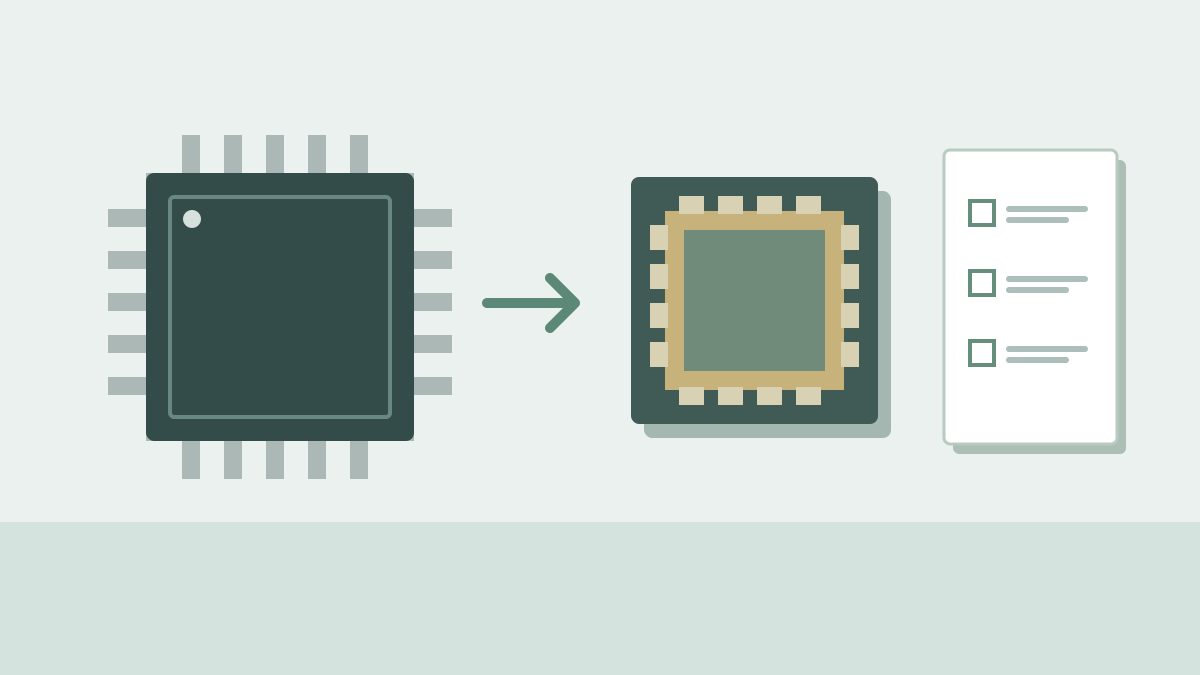
Moving an IC design from QFP to QFN requires a function-by-function comparison of the exact parts, followed by schematic, PCB layout, assembly and test changes. Even when both packages contain the same IC family, they may have different terminal counts, available I/O, land patterns and exposed-pad requirements.
The practical question is: Can the exact alternative orderable part perform the required functions on a redesigned board, and can the team build, test and support it?
The MSP430FR2355 example below illustrates a redesign decision; it does not imply that the two packages are pin-compatible.
Start with the exact orderable parts
For the TI MSP430FR2355 example:
| Orderable part | Package | Terminals | Approximate package body |
|---|---|---|---|
MSP430FR2355TPT |
LQFP | 48 | 7 × 7 mm |
MSP430FR2355TRHAR |
VQFN | 40 | 6 × 6 mm |
PT and RHA identify the respective package drawings. Other orderable variants may use different packing suffixes; check the complete order code and current ordering information. The body dimensions above are approximate; use the controlled mechanical drawings for dimensions and tolerances. The terminal counts differ, and the package choice changes I/O availability. Do not substitute one footprint for the other or assume matching pin numbers. The Texas Instruments MSP430FR235x/MSP430FR215x datasheet, SLASEC4D, specifies connecting the RHA exposed pad to VSS; its package drawing calls for soldering the thermal pad to the PCB for thermal and mechanical performance.
The package dimensions and exposed-pad requirement establish a useful comparison, but they do not establish a releasable design. This example does not provide a verified terminal-by-terminal migration map, a package-specific usable-I/O count, or live ordering status. Those remain release checks, not assumptions. Record the controlled datasheet revision used for the work and confirm the current ordering and lifecycle status of each full MPN before committing to a build.
When the package change introduces a proposed alternate MPN, include it in the project's component substitution approval process. A parts approval does not replace the board redesign and qualification described below.
Using the approximate body dimensions gives 49 mm² for the LQFP and 36 mm² for the VQFN. That is an approximate body-area reduction of 26.5%, but it is not a prediction of the board area saved.
Build the migration map before drawing the new footprint
Begin with the existing product’s actual requirements: power, ground, clocks, programming, debugging, interfaces, analog functions and every used GPIO. Include functions that are needed only during manufacturing, service or fault recovery.
Then compare the top-view terminal maps and device tables for the exact packages in the controlled TI datasheet. A useful working table has one row per required function:
The following two rows are a partial example, based on Table 4-1 of SLASEC4D for these package options:
| Signal or function | PT LQFP terminal | RHA VQFN terminal | Migration decision |
|---|---|---|---|
TEST/SBWTCK |
4 | 3 | Move the programming and debug connection to the RHA terminal and verify access with the actual programming interface. |
P6.6/TB3CLK |
16 | Not listed for RHA | If the product uses this pin or function, assess the requirement and possible alternatives before accepting the package change. |
The dash in the RHA column of the datasheet means this particular pin entry is not available on that package. It does not, by itself, determine whether another pin or peripheral can satisfy the product's requirement. Verify pin multiplexing, firmware, electrical limits and the complete set of connections for the actual design.
Build the complete project mapping separately:
| Required function or connection | Existing LQFP terminal and use | Proposed VQFN terminal and use | Evidence and disposition |
|---|---|---|---|
| Each product I/O and peripheral signal | Enter verified terminal and selected function | Enter verified terminal and selected function, or mark unavailable | Check multiplexing, electrical limits and firmware configuration |
| Supply, VSS and other required connections | Enter verified terminals and schematic treatment | Enter verified terminals and schematic treatment | Check all required connections against the datasheet |
| Programming, debug and manufacturing access | Enter actual connections and test access | Enter proposed connections and test access | Confirm fixtures and software still work |
| VQFN exposed pad | No one-to-one terminal equivalence assumed | Exposed pad: connect to VSS | Implement and review the board connection |
The table is a method, not a completed pin map. Fill in terminal identifiers only after checking the actual package diagrams and tables. Count the I/O that remains available after reserving the product’s required functions; a headline terminal count cannot answer that question.
If a required signal is unavailable, a peripheral function conflicts with another assigned function, or the remaining test access is inadequate, the VQFN proposal needs an explicit design change—or it stops. Do not hide that decision in a CAD-library update.
Change the schematic as well as the layout
Give the alternative package its correct symbol, MPN and package assignment. Check power and ground connections, unused-pin treatment, configuration requirements, decoupling and interface constraints against the controlled datasheet. Compare the existing firmware’s pin configuration with the proposed allocation, including startup behavior and programming access.
For the VQFN, show the exposed-pad-to-VSS connection in the design data clearly enough that it cannot be lost between schematic and layout. The RHA package also has a separate DVSS terminal at pin 6; do not use the exposed pad as a substitute for that connection. Review the electrical net, copper connection and fabrication outputs together. A pad that exists in the footprint but is electrically isolated does not meet the stated requirement.
Run schematic and PCB design-rule checks, but do not treat a clean automated report as proof that the migration map is correct. A reviewer should independently compare the symbol, map and layout to the package documents.
Compare the exact footprint and usable board area
A QFP has leads extending from its body. A QFN has contacts under and around the package edge, and this VQFN also has an exposed pad. For either part, build or verify the footprint against the applicable package drawing and land-pattern guidance, then check:
- Terminal pitch, pad positions and numbering, including orientation and pin-one marking
- Solder-mask openings, paste apertures, courtyard and component keepouts
- Exposed-pad dimensions and its connection to VSS
- Via placement, routing access and any restrictions imposed by the assembly process
- Silkscreen and polarity marks that remain useful after assembly
Use the actual footprint and assembly constraints to compare board occupancy. Body size alone excludes QFP lead lands and may omit the space needed for QFN routing, thermal copper or inspection.
For example, suppose a different hypothetical comparison gives a QFP an 11 × 11 mm reserved layout envelope and a QFN a 9 × 10 mm envelope. The arithmetic is:
- QFP envelope: 121 mm²
- QFN envelope: 90 mm²
- Difference: 31 mm², or about 25.6% of the QFP envelope
These are illustrative layout assumptions, not dimensions for the MSP430 packages. Even that 31 mm² is not automatically usable component space: trace escape, neighboring clearances and thermal copper may still occupy it. Compare placement and routing in the actual board context.
Design and verify the thermal path
The VQFN exposed pad is both an electrical requirement and a potential heat-transfer path. Connect it to VSS as specified, then assess how heat reaches surrounding copper and, if appropriate, other layers through vias. Via geometry and treatment must also suit the assembly process; an unsuitable design can affect paste behavior or solder flow.
Do not assume the VQFN is thermally better simply because it has an exposed pad. Heat dissipation depends on the device’s power, copper geometry, stackup, airflow and operating conditions. Likewise, visible QFP leads do not by themselves establish a thermal limit.
Set acceptance criteria for the product’s worst credible operating conditions. Use analysis where appropriate, then measure representative prototype hardware. If pad voiding is part of the thermal or reliability risk, agree on how it will be assessed and what evidence is acceptable for this design.
Plan assembly, inspection and rework together
The leadless package may reduce placement area, while its underside joints and exposed pad require a carefully developed attachment process. Review land pattern, stencil design, paste deposit, placement and reflow as a system. For the exposed pad, paste-aperture division and coverage should be chosen for the device and process, not copied as a universal percentage.
QFP leads provide visible features that can help inspection, but appearance alone does not prove every joint is sound. QFP assembly can also present lead-alignment or solder-bridging concerns. QFN inspection access depends on the package and board design; hidden interfaces may require additional evidence.
Choose inspection methods from the actual risk and acceptance requirements. Visual inspection, automated optical inspection, electrical testing and X-ray may each contribute evidence, but X-ray is not automatically mandatory for every QFN build. Agree in advance on what each method can and cannot establish.
An assembly inspection report can record the methods used, their coverage, results and any exceptions for the revised board.
Rework deserves its own trial or documented assessment. Consider removal heat, neighboring parts, pad damage, cleaning, replacement, exposed-pad soldering and post-rework verification. Neither package should be declared universally easy or impossible to rework. Ask the intended assembly and service teams to assess the actual board rather than assuming a supplier has a particular capability.
For the broader decision between PCB rework and rebuild, compare the expected repair process and verification requirements with the value and condition of the assembly.
Cost is conditional too. Part pricing, supply, stencil or process changes, inspection, yield, board area, test coverage and field support can all affect the result. For a PCB assembly project, request a build-specific assessment through the quote page, including the exact MPNs, drawings, quantities and acceptance needs. Confirm the agreed process and inspection scope for the order. For broader package context, see circuit board components.
Protect test coverage and qualify the change
A smaller package can remove or relocate convenient probe access even if the required product functions still fit. Compare the current and proposed test strategies:
- Confirm power, ground, programming and debug access on the redesigned board.
- Review fixture contacts, test pads and clearances after placement and routing.
- Check that manufacturing tests detect opens, shorts and relevant assembly faults.
- Re-run functional tests with the firmware and pin configuration intended for release.
- Document any lost coverage and the alternative evidence or risk acceptance.
Build prototype or first-build hardware before volume release. Inspect it using the agreed plan, verify programming and interfaces, and test electrical and thermal behavior under relevant operating conditions. Qualification should reflect the product’s environment and applicable reliability, safety and regulatory obligations; a package change does not have one universal test list.
If firmware, fixtures or manufacturing instructions change, qualify those changes alongside the board. A mechanically successful build is not sufficient if the product cannot be programmed, tested or serviced.
Decision matrix: keep, redesign or stop
Use this matrix as a set of gates, not a weighted score. A space advantage cannot compensate for a missing required function.
| Decision area | Evidence that favors proceeding with VQFN | Response if evidence is missing or unfavorable |
|---|---|---|
| Function fit | Verified map covers every required signal, supply and access function without unresolved conflicts | Redesign the function allocation or retain LQFP |
| Physical fit | Actual footprint, routing and keepouts create a useful layout benefit | Keep LQFP if the body-size saving does not translate into a product benefit |
| Thermal and electrical | VSS pad connection is correct; analysis and prototype results meet limits | Revise copper, stackup or operating assumptions and retest |
| Build and inspection | Process and acceptance plan provide adequate joint-quality evidence | Develop the process or choose the package supported by the evidence |
| Test and service | Programming, fault coverage and rework approach remain acceptable | Add access or procedures; stop if coverage cannot be restored or accepted |
| Supply and lifecycle | Current status and procurement plan support the release quantity and schedule | Resolve sourcing risk before approval |
| Change impact | Firmware, documentation, qualification and ownership are funded and approved | Defer the change or retain the existing design |
For this example, the responsible decision is hold pending verification, not an automatic VQFN selection. The available facts justify investigating the alternative; they do not establish the completed map, live supply status or product-specific qualification.
Change-release checklist
Assign an owner to each item and retain the evidence with the change record. A PCB assembly engineering change order can connect the approved board, BOM, test and manufacturing revisions to the intended production cut-in.
- Engineering: Record full MPNs, package identifiers and controlled datasheet revision; verify current ordering and lifecycle status.
- System and electrical: Approve the completed terminal/function map, usable-I/O assessment and any changed requirements.
- CAD and layout: Release reviewed symbols, footprints, net connections, fabrication outputs and assembly drawings. Verify the VQFN exposed pad is connected to VSS.
- Firmware and test: Approve pin configuration, programming, fixtures, test coverage and any revised procedures.
- Manufacturing and quality: Approve the assembly, inspection, rework and acceptance plans for the actual board.
- Qualification owner: Review prototype or first-build electrical, thermal, functional and reliability evidence against the project’s criteria.
- Change owner: Update the BOM, board revision, approved parts, traceability and service documentation; obtain required cross-functional approvals before release.
A rejected or deferred change is still a valid outcome. Record why, so a future team does not repeat the same assumptions.
FAQ
Is a QFN always smaller than a QFP?
No. Package families contain many sizes. Compare the exact body, lands, courtyard, routing and keepouts for the two orderable parts. A smaller body may not create an equivalent amount of usable board space.
Can I replace the example LQFP with the VQFN by changing only the footprint?
No. The example parts have different terminal counts and I/O availability, and the VQFN exposed pad must connect to VSS. A verified function map, schematic changes, layout redesign and qualification are required.
Does an exposed pad guarantee better thermal performance?
No. It can provide a heat-transfer path, but actual performance depends on the board, power and environment. Design the copper path and verify temperatures against the product’s limits.
Is X-ray required for every QFN assembly?
Not universally. Select inspection and test methods according to joint visibility, risk, acceptance criteria and the evidence needed for the particular assembly process.
What if the VQFN has too few usable I/O functions?
Do not release it as a direct replacement. Assess whether a documented product, firmware or architecture change can meet the requirements; otherwise retain the suitable LQFP or evaluate another device.