
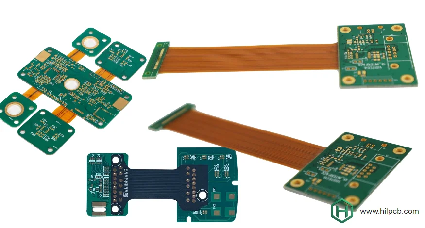
As a measurement and consistency validation engineer focused on TDR/VNA measurement and S-parameter extraction, I know that in today’s ultra-high-speed, high-density electronic design, interconnect technology selection can make or break the system. Among PCB technologies, Rigid-flex PCB stands out with unique 3D routing and strong reliability, becoming a core approach to solve complex high-speed SI challenges. It is not only a circuit carrier—it is a key enabler of end-to-end channel consistency from chip to connector.
From an SI validation perspective, this article explains the key advantages and challenges of Rigid-flex PCB in high-speed design, and how advanced materials, stackup design, and manufacturing processes can address attenuation, crosstalk, and impedance discontinuities at 28G, 56G, and even 112G+ data rates. We focus on Hybrid stackups, Microvia/stacked via, surface finish, backdrill control, and innovative thermal solutions—practical engineering choices that drive high-performance Rigid-flex PCB.
Why Rigid-flex PCB is a key choice for high-speed design
Traditionally, rigid boards are interconnected via cables and connectors. As data rates rise to multi-Gbps, these discrete interfaces introduce significant impedance discontinuities and become major sources of reflections and loss. Every conversion (board–connector–cable–connector–board) is like a speed bump on a highway, compressing eye opening and consuming jitter budget.
Rigid-flex PCB integrates rigid and flex regions seamlessly and eliminates these mechanical interconnect interfaces. Key benefits include:
Superior signal integrity: continuous etched copper paths remove connector mismatch points, reducing insertion loss and return loss and providing a cleaner channel for high-speed SerDes. In TDR measurements, a well-designed rigid-flex transition shows much smaller impedance variation than connector-based solutions.
3D packaging and high-density integration: flex regions allow folding/bending in 3D to fit compact products (wearables, avionics, high-end servers). Designers can integrate multiple rigid functions into a single Rigid-flex PCB, shortening critical paths and reducing interlayer coupling risk.
Higher reliability: eliminating connector failure points (vibration loosening, contact intermittency) improves long-term reliability in harsh environments—critical for aerospace, medical, and automotive electronics.
Simplified assembly and lower total cost: although single-board Rigid-flex PCB fabrication is more expensive, the reduced connectors/cables and manual assembly can lower TCO and increase FPY.
Optimizing SI and cost with Hybrid stackup
In ultra-high-speed digital, material Dk and Df strongly determine attenuation. Ideally, you would use ultra-low-loss materials everywhere (Rogers, Megtron), but cost is high; for systems with large low-speed/control and power plane areas, full-board premium material is often not economical.
Hybrid stack-up (Rogers+FR-4) addresses this by combining high-performance materials and standard FR-4 strategically based on region/layer requirements:
- High-speed signal layers: layers carrying critical differential pairs (PCIe, Ethernet, SerDes) use Rogers RO4350B/RO4835, Tachyon 100G, or similar low Dk/Df materials to minimize loss and dispersion.
- Power and low-speed layers: power/ground planes and low-speed control layers use cost-effective FR-4 such as High-Tg FR-4 to meet basic electrical/thermal needs.
When implementing Hybrid stack-up (Rogers+FR-4), validation engineers should watch:
- Stackup symmetry: symmetry is required to avoid warpage; asymmetric material combinations create CTE mismatch and stress during reflow.
- Material compatibility: different materials have different resin flow/cure and pressure windows; experienced mixed-lamination processing is needed to prevent delamination/voids.
- Impedance modeling accuracy: impedance models must use correct frequency-specific Dk/Df for each material; using generic values causes errors and hurts impedance control accuracy.
With careful Hybrid stack-up (Rogers+FR-4), you can significantly optimize high-speed PCB cost without sacrificing key channel performance.
Hybrid stackup: performance vs cost comparison
| Stackup option | Typical use | Signal integrity | Relative cost | Manufacturing complexity |
|---|---|---|---|---|
| All FR-4 | < 5 Gbps | Moderate | ★ | Low |
| Hybrid stack-up (Rogers+FR-4) | 5 - 56 Gbps | Excellent | ★★★ | High |
| All Rogers/Megtron | > 56 Gbps / RF | Best-in-class | ★★★★★ | Medium |
Microvia/stacked via in Rigid-flex PCB
As BGA pitch shrinks to 0.5mm and below, traditional mechanical through-holes cannot meet routing density. HDI—especially Microvia/stacked via—becomes standard in Rigid-flex PCB.
- Microvia: typically laser vias <150µm (6 mil) connecting adjacent layers. Smaller pads create fanout space and can reduce overall layer count. From SI perspective, parasitic C/L are much lower than through-holes.
- Stacked via: stacking multiple microvias vertically creates a direct interconnect channel. It shortens paths and avoids extra routing required by staggered vias—ideal for direct high-speed layer transitions.
Applying Microvia/stacked via requires high-precision laser drilling and plated-filled capabilities. Reliability is critical: plating defects can create opens, so strict process control and microsection analysis are needed. Experienced manufacturers like HILPCB can ensure electrical performance and long-term reliability, which is essential for HDI PCB.
Unique SI challenges in flex regions
The flex transition and bending zones are the most challenging areas: different materials, geometry, and mechanical stress introduce unique SI problems.
Harder impedance control: flex substrates (Polyimide) and Coverlay have larger thickness tolerance and no fiberglass reinforcement; Dk uniformity is worse than rigid materials. Use wider traces, tighter etch control, and careful 2D field-solver modeling.
Bending impact: when flex bends, outer traces stretch and inner traces compress, changing physical length and cross-section, shifting impedance and delay. Differential pairs must keep bend radius and path length symmetric after bending to avoid mode conversion (differential-to-common). Placing traces on the Neutral Axis minimizes bending stress.
Reference plane discontinuity: flex areas often use hatched ground rather than solid planes for flexibility. That breaks return paths, increases loop inductance, and can worsen crosstalk/EMI. Optimize hatch density/geometry to balance SI and mechanical flexibility.
🌀 Flex zone: high-speed SI & reliability design matrix
Enforce Circular Traces in bending areas. Avoid 90°/45° corners to eliminate stress concentration and minimize reflection/impedance discontinuities in the bend.
Add Teardrop at pad-trace junctions to increase bonding area and distribute mechanical stress during dynamic bending, reducing pad-edge trace breaks.
Precisely place FR-4 or PI stiffeners at connectors and SMT areas to locally rigidize the flex and prevent assembly stress from reaching sensitive solder joints.
Avoid vias in the Bending Radius zone. Vias break Polyimide continuity and become micro-crack initiation sites. Move layer transitions to rigid zones or stiffened static zones.
To prevent twist in flex fabrication (I-Beam Effect), we recommend Staggered Traces between top and bottom layers. Combined with HILPCB precision vacuum lamination, impedance variation can stay very low even after millions of bend cycles.
How surface finish impacts high-speed transmission
Surface finish is not only for copper protection and solderability; it can affect high-speed loss, especially at mmWave frequencies, through surface roughness and Skin Effect.
- OSP: a thin organic film with very smooth copper surface. It often yields the lowest insertion loss at high frequency, but has limited thermal robustness and reflow cycles.
- ENIG: widely used; flat and solderable. But its nickel layer (typically 3–6µm) adds resistivity/magnetic loss and can increase insertion loss at high frequency, especially above 10GHz—needs careful evaluation for ultra-high-speed.
- ENEPIG: adds a palladium layer on top of ENIG to reduce nickel migration (black pad) and improve solder joint reliability; SI impact is similar to ENIG due to nickel.
For 28Gbps and above, prefer high-frequency-friendly finishes such as OSP or Immersion Gold without nickel, when feasible. When choosing ENIG/ENEPIG/OSP, you must balance SI, cost, reliability, and process windows. For wire-bond applications, ENIG/ENEPIG may be required; then compensate via stackup/routing optimization.
Backdrill quality control for high-speed links
Above ~10Gbps, via stubs become a major SI problem. The unused via segment behaves like an open transmission line and resonates (quarter-wave), creating deep notches in S21 (insertion loss).
Backdrilling (Controlled Depth Drilling) removes excess stubs from the backside. Backdrill quality control is critical to ensure channel performance.
Ideal backdrill removes stubs as close to the signal layer as possible, leaving only a small residual (often <10 mil) for reliability. Accurate Backdrill quality control depends on:
- Precise Z-depth control: drill depth tolerance typically within ±2 mil.
- Reliable residual stub measurement: validate with TDR profiling or microsection analysis. TDR provides non-destructive impedance profiles and clearly shows stub impact.
Without strict backdrill control, you can over-drill into signal layers and cause link failure. Choosing a manufacturer like HILPCB with mature backdrill processes and validation capability reduces risk.
HILPCB high-precision manufacturing capability
Max layer count
64L (Rigid), 20L (Rigid-flex)
Min trace/space
2.5 / 2.5 mil
Impedance tolerance
±5%
Backdrill depth tolerance
±0.05mm
Solving local thermal issues with Copper coin
As chip power density increases, thermal management becomes another major challenge—especially in compact spaces where heatsinks/fans are limited. Copper coin provides an efficient embedded thermal solution.
Copper coin embeds a solid copper block (round, square, etc.) into the PCB lamination. The coin contacts the thermal pad of heat sources (FPGA, CPU, power devices) and uses Thermal Vias to quickly conduct heat to the opposite side or internal thermal planes.
Benefits:
- Very high thermal conductivity: copper (
400 W/m·K) far exceeds PCB base materials (0.3 W/m·K), creating an efficient vertical thermal path. - Embedded integration: fully internal; does not consume extra volume—ideal for space-constrained designs.
- Structural stability: laminated together, forming a robust structure.
In Rigid-flex PCB, Copper coin requires precise thickness/placement control to ensure seamless bonding to surrounding dielectric/copper layers and avoid delamination/voids—an advanced process that demands strong lamination and CNC capabilities.
How HILPCB ensures Rigid-flex PCB manufacturing and test consistency
Between theoretical design and final performance sits manufacturing reality. As a leading solution provider, HILPCB uses complete DFM review, advanced processes, and strict validation so each Rigid-flex PCB meets demanding high-speed performance.
- Early DFM and simulation support: review stackup (including Hybrid stack-up (Rogers+FR-4)), materials, impedance planning, and flex-zone design; use simulation to predict SI/PI/thermal and fix issues early.
- Precision process control: high-end equipment for Microvia/stacked via, strict Backdrill quality control, and stable production of ENIG/ENEPIG/OSP finishes.
- Measurement and validation: beyond AOI and electrical test, HILPCB uses VNA and high-bandwidth TDR to provide S-parameter reports and impedance coupons—verifying loss, crosstalk, and impedance match simulation and spec.
- One-stop service: from PCB manufacturing to SMT assembly and functional testing, ensuring supply-chain quality and speed for fast time-to-market.
Conclusion
Rigid-flex PCB is no longer a niche specialty—it is a mainstream technology for miniaturization, integration, and high-speed challenges in modern electronics. Success requires deep understanding across materials, EM theory, and manufacturing. By strategically applying Hybrid stack-up (Rogers+FR-4), Microvia/stacked via, optimized finishes (ENIG/ENEPIG/OSP), strict Backdrill quality control, and innovative Copper coin thermal design, you can break traditional PCB performance limits.
Partnering with an experienced, technology-leading manufacturer like HILPCB is key to turning complex rigid-flex designs into high-performance products. We combine advanced manufacturing with strict validation to help you win in a competitive market.
Common Questions
Why is high-speed signal integrity more difficult on rigid-flex PCBs?
Rigid-flex designs combine impedance-sensitive routing with mechanical bending, mixed materials, and complex transitions between rigid and flex zones. Those factors make loss, skew, stub control, and return-path continuity harder to manage than on a simple rigid board.
When is backdrilling necessary in a rigid-flex high-speed design?
Backdrilling becomes important when via stubs are long enough to hurt insertion loss or create resonances, especially above roughly 10 Gbps. It is typically evaluated together with stack-up, layer transitions, and channel budget targets.
Which surface finish is usually better for very high-speed rigid-flex channels?
There is no single answer, but finishes with smoother copper interfaces and no nickel layer are often preferred for lower loss. The final choice must balance signal integrity, assembly reliability, reflow robustness, and product cost.
Can thermal management and signal integrity be solved together in rigid-flex systems?
Yes, but they need to be designed together from the beginning. Features such as copper coin structures, hybrid stack-ups, and controlled flex geometry can improve thermal performance without sacrificing high-speed electrical behavior when the manufacturing process supports them.